SI824XCLASSD-KIT Silicon Laboratories Inc, SI824XCLASSD-KIT Datasheet - Page 20
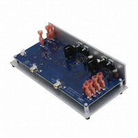
SI824XCLASSD-KIT
Manufacturer Part Number
SI824XCLASSD-KIT
Description
BOARD EVAL FOR SI824X
Manufacturer
Silicon Laboratories Inc
Datasheet
1.SI8241CB-B-IS1.pdf
(30 pages)
Specifications of SI824XCLASSD-KIT
New! Us2012 Catalog Page
Class-D Audio Driver_Precision Clock ICs
Board Type
Fully Populated
Amplifier Type
Class D
Output Type
2-Channel (Stereo)
Max Output Power X Channels @ Load
120W x 2 @ 8 Ohm
Utilized Ic / Part
Si824x
Description/function
Audio Amplifiers
Operating Supply Voltage
12 V
Output Power
30 W to 1000 W
Product
Audio Development Tools
Supply Current
500 mA
For Use With/related Products
Si824x
Lead Free Status / RoHS Status
Lead free / RoHS Compliant
Voltage - Supply
-
Operating Temperature
-
Lead Free Status / RoHS Status
Lead free / RoHS Compliant
Other names
336-2002


Si824x
3.6. Layout Considerations
It is most important to minimize ringing in the drive path and noise on the Si824x VDD lines. Care must be taken to
minimize parasitic inductance in these paths by locating the Si824x as close to the device it is driving as possible.
In addition, the VDD supply and ground trace paths must be kept short. For this reason, the use of power and
ground planes is highly recommended. A split ground plane system having separate ground and VDD planes for
power devices and small signal components provides the best overall noise performance.
3.7. Undervoltage Lockout Operation
Device behavior during start-up, normal operation and shutdown is shown in Figure 33, where UVLO+ and UVLO-
are the positive-going and negative-going thresholds respectively. Note that outputs VOA and VOB default low
when input side power supply (VDDI) is not present.
3.7.1. Device Startup
Outputs VOA and VOB are held low during power-up until VDD is above the UVLO threshold for time period
tSTART. Following this, the outputs follow the states of inputs VIA and VIB.
3.7.2. Undervoltage Lockout
Undervoltage Lockout (UVLO) is provided to prevent erroneous operation during device startup and shutdown or
when VDD is below its specified operating circuits range. The input (control) side, Driver A and Driver B, each have
their own undervoltage lockout monitors.
The Si824x input side enters UVLO when VDDI < VDDI
outputs, VOA and VOB, remain low when the input side of the Si824x is in UVLO and their respective VDD supply
(VDDA, VDDB) is within tolerance. Each driver output can enter or exit UVLO independently. For example, VOA
unconditionally enters UVLO when VDDA falls below VDDA
VDDA
20
DISABLE
UVLO+
VDDI
UVLO-
UVLO+
VDDA
PW M
UVLO-
VOA
UV+
tSTART
.
VDD
VDD
Figure 33. Device Behavior during Normal Operation and Shutdown
HYS
HYS
tSD
tSTART
tSTART
Rev. 0.2
UV–
tSD
, and exits UVLO when VDDI > VDDI
UV–
tRESTART
and exits UVLO when VDDA rises above
tPHL
tPLH
UV+
. The driver
Related parts for SI824XCLASSD-KIT
Image
Part Number
Description
Manufacturer
Datasheet
Request
R

Part Number:
Description:
SMD/C°/SINGLE-ENDED OUTPUT SILICON OSCILLATOR
Manufacturer:
Silicon Laboratories Inc
Part Number:
Description:
Manufacturer:
Silicon Laboratories Inc
Datasheet:
Part Number:
Description:
N/A N/A/SI4010 AES KEYFOB DEMO WITH LCD RX
Manufacturer:
Silicon Laboratories Inc
Datasheet:
Part Number:
Description:
N/A N/A/SI4010 SIMPLIFIED KEY FOB DEMO WITH LED RX
Manufacturer:
Silicon Laboratories Inc
Datasheet:
Part Number:
Description:
N/A/-40 TO 85 OC/EZLINK MODULE; F930/4432 HIGH BAND (REV E/B1)
Manufacturer:
Silicon Laboratories Inc
Part Number:
Description:
EZLink Module; F930/4432 Low Band (rev e/B1)
Manufacturer:
Silicon Laboratories Inc
Part Number:
Description:
I°/4460 10 DBM RADIO TEST CARD 434 MHZ
Manufacturer:
Silicon Laboratories Inc
Part Number:
Description:
I°/4461 14 DBM RADIO TEST CARD 868 MHZ
Manufacturer:
Silicon Laboratories Inc
Part Number:
Description:
I°/4463 20 DBM RFSWITCH RADIO TEST CARD 460 MHZ
Manufacturer:
Silicon Laboratories Inc
Part Number:
Description:
I°/4463 20 DBM RADIO TEST CARD 868 MHZ
Manufacturer:
Silicon Laboratories Inc
Part Number:
Description:
I°/4463 27 DBM RADIO TEST CARD 868 MHZ
Manufacturer:
Silicon Laboratories Inc
Part Number:
Description:
I°/4463 SKYWORKS 30 DBM RADIO TEST CARD 915 MHZ
Manufacturer:
Silicon Laboratories Inc
Part Number:
Description:
N/A N/A/-40 TO 85 OC/4463 RFMD 30 DBM RADIO TEST CARD 915 MHZ
Manufacturer:
Silicon Laboratories Inc
Part Number:
Description:
I°/4463 20 DBM RADIO TEST CARD 169 MHZ
Manufacturer:
Silicon Laboratories Inc