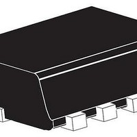
ZXSDS2M832TA Diodes Inc, ZXSDS2M832TA Datasheet - Page 2

ZXSDS2M832TA
Manufacturer Part Number
ZXSDS2M832TA
Description
Schottky (Diodes & Rectifiers) VR=60V IF=1.65A IR=100uA
Manufacturer
Diodes Inc
Datasheet
1.ZXSDS2M832TA.pdf
(6 pages)
Specifications of ZXSDS2M832TA
Product
Schottky Diodes
Peak Reverse Voltage
60 V
Forward Continuous Current
1.24 A
Max Surge Current
16.8 A
Configuration
Dual Parallel
Recovery Time
12 ns
Forward Voltage Drop
0.74 V at 1.5 A
Maximum Reverse Leakage Current
100 uA at 45 V
Operating Temperature Range
- 55 C to + 125 C
Mounting Style
SMD/SMT
Package / Case
MLP-832
Lead Free Status / RoHS Status
Lead free / RoHS Compliant
ABSOLUTE MAXIMUM RATINGS
THERMAL RESISTANCE
NOTES
(a) For a dual device surface mounted on 8 sq. cm single sided 2oz copper on FR4 PCB, in still air conditions with all exposed pads attached. The
(b) Measured at t<5 secs for a dual device surface mounted on 8 sq cm single sided 2oz copper on FR4 PCB, in still air conditions with all exposed
(c) For a dual device surface mounted on 8 sq cm single sided 2oz copper FR4 PCB, in still air conditions with minimal lead connections only.
(d) For a dual device surface mounted on 10 sq cm single sided 1oz copper FR4 PCB, in still air conditions with all exposed pads attached. The
(e) For a dual device surface mounted on 85 sq cm single sided 2oz copper FR4 PCB, in still air conditions with all exposed pads attached. The
(f) For dual device with one active die.
(g) For dual device with 2 active die running at equal power.
(h) Repetitive rating - pulse width limited by max junction temperature. Refer to Transient Thermal Impedance graph.
(i) The minimum copper dimensions required for mounting are no smaller than the exposed metal pads on the base of the device as shown in
ZXSDS2M832
PARAMETER
Reverse Voltage
Forward Voltage @ I
Forward Current
Average Forward Current D=50%, t<=300us
Non Repetitive Forward Current t<=100us
Non Repetitive Forward Current t<=10ms
Power Dissipation at TA=25°C
Linear Derating Factor
Power Dissipation at TA=25°C
Linear Derating Factor
Power Dissipation at TA=25°C
Linear Derating Factor
Power Dissipation at TA=25°C
Linear Derating Factor
Power Dissipation at TA=25°C
Linear Derating Factor
Power Dissipation at TA=25°C
Linear Derating Factor
Storage Temp, Range
Operating & Storage Temp, Range
PARAMETER
Junction to Ambient
Junction to Ambient
Junction to Ambient
Junction to Ambient
Junction to Ambient
Junction to Ambient
copper area is split down the center line into two separate areas with one half connected to each half of the dual device.
pads attached. The copper area is split down the centerline into two separate areas with one half connected to each half of the dual device.
copper area is split down the centerline into two separate areas with one half connected to each half of the dual device.
copper area is split down the centerline into two separate areas with one half connected to each half of the dual device.
the package dimensions data. The thermal resistance for a dual device mounted on 1.5mm thick FR4 board using minimum copper of 1 oz
weight, 1mm wide tracks and one half of the device active is Rth= 250°C/W giving a power rating of Ptot=400mW.
S E M I C O N D U C T O R S
F
(a)(f)
(b)(f)
(c)(f)
(d)(f)
(d)(g)
(e)(g)
= 1000mA
(b)(f)
(d)(f)
(a)(f)
(c)(f)
(d)(g)
(e)(g)
OBSOLETE
SYMBOL
V
V
I
I
I
P
P
P
P
P
P
Tstg
Tj
SYMBOL
R JA
R JA
R JA
R JA
R JA
R JA
F
FAV
FSM
2
D
D
D
D
D
D
R
F
-55 to+150
-55 to+125
VALUE
LIMIT
83.3
73.5
41.7
1.65
1.24
16.8
5.63
1.36
13.6
125
111
600
1.2
0.8
0.9
2.4
51
60
12
20
24
2
8
9
ISSUE 2 June 2003
mW/°C
mW/°C
mW/°C
mW/°C
mW/°C
mW/°C
UNIT
°C/W
°C/W
°C/W
°C/W
°C/W
°C/W
UNIT
mV
W
W
W
W
W
W
°C
°C
V
A
A
A
A


