MMBD352WT1 ON Semiconductor, MMBD352WT1 Datasheet

Schottky (Diodes & Rectifiers) 7V 225mW Dual

MMBD352WT1

Manufacturer Part Number
MMBD352WT1
Description
Schottky (Diodes & Rectifiers) 7V 225mW Dual
Manufacturer
ON Semiconductor
Datasheet

Specifications of MMBD352WT1

Product
Schottky Diodes
Peak Reverse Voltage
7 V
Configuration
Dual Series
Forward Voltage Drop
0.6 V @ 0.01 A
Maximum Reverse Leakage Current
10 uA
Operating Temperature Range
- 55 C to + 150 C
Mounting Style
SMD/SMT
Package / Case
SC-70
Lead Free Status / RoHS Status
Lead free / RoHS Compliant

Available stocks

Company
Part Number
Manufacturer
Quantity
Price
Part Number:
MMBD352WT1G
Manufacturer:
ON
Quantity:
30 000
MMBD352WT1G
Dual Schottky Barrier Diode
but are suitable also for use in detector and ultra- -fast switching
circuits.
Features
Stresses exceeding Maximum Ratings may damage the device. Maximum
Ratings are stress ratings only. Functional operation above the Recommended
Operating Conditions is not implied. Extended exposure to stresses above the
Recommended Operating Conditions may affect device reliability.
1. FR-- 5 = 1.0 ¢ 0.75 ¢ 0.062 in.
2. Alumina = 0.4 ¢ 0.3 ¢ 0.024 in. 99.5% alumina.
 Semiconductor Components Industries, LLC, 2010
October, 2010 - - Rev. 4
MAXIMUM RATINGS
THERMAL CHARACTERISTICS
Continuous Reverse Voltage
Total Device Dissipation FR-- 5 Board
Thermal Resistance,
Total Device Dissipation Alumina
Thermal Resistance,
Junction and Storage Temperature
These devices are designed primarily for UHF mixer applications
Compliant
Very Low Capacitance - - Less Than 1.0 pF @ 0 V
Low Forward Voltage - - 0.5 V (Typ) @ I
These Devices are Pb- -Free, Halogen Free/BFR Free and are RoHS
(Note 1)
T
Derate above 25C
Junction--to--Ambient
Substrate (Note 2) T
Derate above 25C
Junction--to--Ambient
A
= 25C
Characteristic
Rating
A
= 25C
Symbol
Symbol
T
R
R
J
V
P
P
, T
θJA
θJA
R
D
D
F
stg
= 10 mA
-- 55 to +150
Value
Max
200
625
300
417
7.0
1.6
2.4
1
mW/C
mW/C
C/W
C/W
Unit
V
Unit
mW
mW
C
CC
†For information on tape and reel specifications,
MMBD352WT1G
including part orientation and tape sizes, please
refer to our Tape and Reel Packaging Specifications
Brochure, BRD8011/D.
Device
(Note: Microdot may be in either location)
1
M5
M
G
ORDERING INFORMATION
ANODE
2
MARKING DIAGRAM
1
http://onsemi.com
CATHODE/ANODE
3
= Specific Device Code
= Date Code
= Pb--Free Package
1
(Pb--Free)
SOT--323
Package
3
M5 MG
Publication Order Number:
SOT- -323 (SC- -70)
G
CASE 419
STYLE 9
3000/Tape & Reel
MMBD352WT1/D
CATHODE
Shipping
2

Related parts for MMBD352WT1

MMBD352WT1 Summary of contents

Page 1

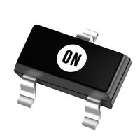
... Microdot may be in either location) ORDERING INFORMATION Device Package Shipping MMBD352WT1G SOT--323 3000/Tape & Reel (Pb--Free) †For information on tape and reel specifications, including part orientation and tape sizes, please refer to our Tape and Reel Packaging Specifications Brochure, BRD8011/D. Publication Order Number: MMBD352WT1/D † ...

Page 2

ELECTRICAL CHARACTERISTICS Characteristic OFF CHARACTERISTICS Forward Voltage ( mAdc) F Reverse Voltage Leakage Current ( Capacitance ( 1.0 MHz) R 100 T = 85C ...

Page 3

... H 2.00 2.10 2.40 0.079 0.083 E PIN 1. ANODE 2. CATHODE 3. CATHODE--ANODE   mm inches ON Semiconductor Website: www.onsemi.com Order Literature: http://www.onsemi.com/orderlit For additional information, please contact your local Sales Representative MMBD352WT1/D MAX 0.040 0.004 0.016 0.010 0.087 0.053 0.055 0.022 0.095 ...

Related keywords