2N5061 ON Semiconductor, 2N5061 Datasheet
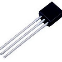
SCRs 50V 800mA Thyristor

2N5061

Manufacturer Part Number
2N5061
Description
SCRs 50V 800mA Thyristor
Manufacturer
ON Semiconductor
Datasheet

Specifications of 2N5061

Breakover Current Ibo Max
10 A
Rated Repetitive Off-state Voltage Vdrm
60 V
Off-state Leakage Current @ Vdrm Idrm
0.01 mA
Forward Voltage Drop
1.7 V
Gate Trigger Voltage (vgt)
0.8 V
Maximum Gate Peak Inverse Voltage
5 V
Gate Trigger Current (igt)
0.2 mA
Holding Current (ih Max)
5 mA
Mounting Style
Through Hole
Package / Case
TO-92-3 (TO-226)
Lead Free Status / RoHS Status
Lead free / RoHS Compliant

Available stocks

Company
Part Number
Manufacturer
Quantity
Price
Part Number:
2N5061
Manufacturer:
FSC
Quantity:
1 550
Part Number:
2N5061
Manufacturer:
ST
0
Part Number:
2N5061
Manufacturer:
台湾
Quantity:
20 000
Part Number:
2N5061G
Manufacturer:
ON
Quantity:
14 277
Part Number:
2N5061G
Manufacturer:
ON
Quantity:
16 722
Part Number:
2N5061RLRAG
Manufacturer:
ON
Quantity:
16 000
2N5060 Series
Sensitive Gate
Silicon Controlled Rectifiers
Reverse Blocking Thyristors
applications such as relay and lamp drivers, small motor controls, gate
drivers for larger thyristors, and sensing and detection circuits.
Supplied in an inexpensive plastic TO−92/TO-226AA package which
is readily adaptable for use in automatic insertion equipment.
Features
*For additional information on our Pb−Free strategy and soldering details, please
© Semiconductor Components Industries, LLC, 2008
November, 2008 − Rev. 9
download the ON Semiconductor Soldering and Mounting Techniques
Reference Manual, SOLDERRM/D.
Annular PNPN devices designed for high volume consumer
T
Sensitive Gate Trigger Current − 200 mA Maximum
Low Reverse and Forward Blocking Current − 50 mA Maximum,
Low Holding Current − 5 mA Maximum
Passivated Surface for Reliability and Uniformity
Device Marking: Device Type, e.g., 2N5060, Date Code
Pb−Free Packages are Available*
C
= 110°C
Preferred Device
1
See detailed ordering and shipping information in the package
dimensions section on page 6 of this data sheet.
Preferred devices are recommended choices for future use
and best overall value.
1 2
1
2
3
SILICON CONTROLLED
3
0.8 A RMS, 30 − 200 V
ORDERING INFORMATION
50xx
Y
WW
A
http://onsemi.com
PIN ASSIGNMENT
RECTIFIERS
STYLE 10
CASE 29
TO−92
Specific Device Code
= Year
= Work Week
Publication Order Number:
Cathode
Anode
Gate
G
MARKING
DIAGRAM
K
2N
50xx
YWW
2N5060/D

Related parts for 2N5061

2N5061 Summary of contents

Page 1

... Device Marking: Device Type, e.g., 2N5060, Date Code • Pb−Free Packages are Available* *For additional information on our Pb−Free strategy and soldering details, please download the ON Semiconductor Soldering and Mounting Techniques Reference Manual, SOLDERRM/D. © Semiconductor Components Industries, LLC, 2008 November, 2008 − Rev. 9 http://onsemi ...

Page 2

... J Rating Peak Repetitive Off−State Voltage (Note *40 to 110°C, Sine Wave Hz kW) 2N5060 GK 2N5061 2N5062 2N5064 On-State Current RMS (180° Conduction Angles; T *Average On-State Current (180° Conduction Angles 67° 102°C) C *Peak Non-repetitive Surge Current 25° ...

Page 3

... T = 25° 110° 25° −40° 25° −40° 25° −40°C C 2N5060, 2N5061 2N5062, 2N5064 RRM RRM Reverse Blocking Region (off state) Reverse Avalanche Region Anode − http://onsemi.com 3 Symbol Min Typ Max DRM RRM − − 10 − − ...

Page 4

CONDUCTION ANGLE 120 110 100 30° 60° 0.1 0.2 0 AVERAGE ON‐STATE CURRENT (AMP) T(AV) Figure 1. Maximum Case Temperature 5.0 3.0 2 110°C J ...

Page 5

T , JUNCTION TEMPERATURE (°C) J Figure 7. Typical Gate Trigger Voltage 4.0 3.0 2.0 1.0 0.8 0.6 ...

Page 6

... ORDERING INFORMATION Device 2N5060 2N5060G 2N5060RLRA 2N5060RLRAG 2N5060RLRM 2N5060RLRMG 2N5061 2N5061G 2N5061RLRA 2N5061RLRAG 2N5062 2N5062G 2N5062RLRA 2N5062RLRAG 2N5064 2N5064RLRA 2N5064RLRM 2N5064RLRMG 2N5064RLRAG 2N5064G †For information on tape and reel specifications, including part orientation and tape sizes, please refer to our Tape and Reel Packaging Specifications Brochure, BRD8011/D ...

Page 7

... Opportunity/Affirmative Action Employer. This literature is subject to all applicable copyright laws and is not for resale in any manner. PUBLICATION ORDERING INFORMATION LITERATURE FULFILLMENT: Literature Distribution Center for ON Semiconductor P.O. Box 5163, Denver, Colorado 80217 USA Phone: 303−675−2175 or 800−344−3860 Toll Free USA/Canada Fax: 303− ...

Related keywords