1N5821G ON Semiconductor, 1N5821G Datasheet - Page 6
1N5821G
Manufacturer Part Number
1N5821G
Description
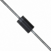
DIODE SCHOTTKY 3A 30V DO-201AD
Manufacturer
ON Semiconductor
Specifications of 1N5821G
Voltage - Forward (vf) (max) @ If
500mV @ 3A
Voltage - Dc Reverse (vr) (max)
30V
Current - Average Rectified (io)
3A
Current - Reverse Leakage @ Vr
2mA @ 30V
Diode Type
Schottky
Speed
Fast Recovery =< 500ns, > 200mA (Io)
Mounting Type
Through Hole
Package / Case
DO-201AD, Axial
Product
Schottky Diodes
Peak Reverse Voltage
30 V
Forward Continuous Current
3 A
Max Surge Current
80 A
Configuration
Single
Forward Voltage Drop
0.9 V @ 9.4 A
Maximum Reverse Leakage Current
2000 uA
Operating Temperature Range
- 65 C to + 125 C
Mounting Style
Through Hole
Current, Forward
3 A
Current, Reverse
20 mA
Current, Surge
80 A
Package Type
DO-201AD
Primary Type
Schottky Barrier
Temperature, Junction, Maximum
+125 °C
Temperature, Operating
-65 to +125 °C
Voltage, Forward
0.5 V
Voltage, Reverse
30 V
Lead Free Status / RoHS Status
Lead free / RoHS Compliant
Reverse Recovery Time (trr)
-
Capacitance @ Vr, F
-
Lead Free Status / Rohs Status
Lead free / RoHS Compliant
Other names
1N5821G
1N5821GOS
1N5821GOS


for the mountings shown is to be used as typical guideline values
for preliminary engineering, or in case the tie point temperature
cannot be measured.
Figure 6. Forward Power Dissipation 1N5820-22
7.0
5.0
3.0
2.0
1.0
0.7
0.5
0.3
0.2
0.1
10
0.1
Data shown for thermal resistance junction-to-ambient (R
Capacitive
Loads
I
SINE WAVE
F(AV)
Mounting
I
I
0.2
Method
(FM)
(AV)
TYPICAL VALUES FOR R
, AVERAGE FORWARD CURRENT (AMP)
1
2
3
NOTE 5 — MOUNTING DATA
+ p (Resistive Load)
0.3
5.0
10
20
0.5
1/8
58
50
Lead Length, L (in)
0.7 1.0
1/4
51
59
28
1/2
53
61
qJA
2.0
IN STILL AIR
3/4
55
63
3.0
SQUARE WAVE
T
J
1N5820, 1N5821, 1N5822
≈ 125°C
°C/W
°C/W
°C/W
R
5.0
qJA
dc
http://onsemi.com
7.0 10
qJA
)
6
resistance for any mounting configuration to be found. For
a given total lead length, lowest values occur when one side
of the rectifier is brought as close as possible to the heat sink.
Terms in the model signify:
T
T
R
R
R
P
P
P
(Subscripts (A) and (K) refer to anode and cathode sides,
respectively.) Values for thermal resistance components
are:
R
R
The maximum lead temperature may be found as follows:
T
where n T
É É É É É É É
É É É É É É É
É É É É É É É É
É É É É É É É É
A
D
F
R
NOTE 4 - APPROXIMATE THERMAL CIRCUIT MODEL
L
L
qS
qL
qJ
qL
qJ
Use of the above model permits junction to lead thermal
= Forward Power Dissipation
= Ambient Temperature
= Lead Temperature
= Total Power Dissipation = P
= Reverse Power Dissipation
= T
= Thermal Resistance, Junction-to-Case
= 10°C/W typically and 16°C/W maximum
= Thermal Resistance, Heatsink to Ambient
= Thermal Resistance, Lead-to-Heatsink
= 42°C/W/in typically and 48°C/W/in maximum
T
R
P.C. Board where available
A(A)
qS(A)
copper surface is small.
J(max)
VECTOR PUSH-IN
Mounting Method 1
Mounting Method 2
TERMINALS T-28
L
T
JL
L
L(A)
* n T
[ R
R
qL(A)
qJL
T
JL
C(A)
L
L
· P
R
qJ(A)
D
T
J
T
É
É
É
É
É
P
R
D
J
qJ(K)
F
= Junction Temperature
T
+ P
C
T
BOARD GROUND
= Case Temperature
C(K)
R
Mounting Method 3
copper surface.
P.C. Board with
2-1/2, x 2-1/2,
L = 1/2″
R
PLANE
qL(K)
T
L(K)
R
T
qS(K)
A(K)
Related parts for 1N5821G
Image
Part Number
Description
Manufacturer
Datasheet
Request
R

Part Number:
Description:
ON Semiconductor [VOLTAGE REGULATOR]
Manufacturer:
ON Semiconductor
Datasheet:
Part Number:
Description:
357-036-542-201 CARDEDGE 36POS DL .156 BLK LOPRO
Manufacturer:
ON Semiconductor
Datasheet:
Part Number:
Description:
357-036-542-201 CARDEDGE 36POS DL .156 BLK LOPRO
Manufacturer:
ON Semiconductor
Datasheet:
Part Number:
Description:
357-036-542-201 CARDEDGE 36POS DL .156 BLK LOPRO
Manufacturer:
ON Semiconductor
Datasheet:
Part Number:
Description:
357-036-542-201 CARDEDGE 36POS DL .156 BLK LOPRO
Manufacturer:
ON Semiconductor
Datasheet:
Part Number:
Description:
357-036-542-201 CARDEDGE 36POS DL .156 BLK LOPRO
Manufacturer:
ON Semiconductor
Datasheet:
Part Number:
Description:
357-036-542-201 CARDEDGE 36POS DL .156 BLK LOPRO
Manufacturer:
ON Semiconductor
Datasheet:
Part Number:
Description:
357-036-542-201 CARDEDGE 36POS DL .156 BLK LOPRO
Manufacturer:
ON Semiconductor
Datasheet:
Part Number:
Description:
357-036-542-201 CARDEDGE 36POS DL .156 BLK LOPRO
Manufacturer:
ON Semiconductor
Datasheet:
Part Number:
Description:
357-036-542-201 CARDEDGE 36POS DL .156 BLK LOPRO
Manufacturer:
ON Semiconductor
Datasheet:
Part Number:
Description:
357-036-542-201 CARDEDGE 36POS DL .156 BLK LOPRO
Manufacturer:
ON Semiconductor
Datasheet:
Part Number:
Description:
Manufacturer:
ON Semiconductor
Datasheet:
Part Number:
Description:
Manufacturer:
ON Semiconductor
Datasheet:
Part Number:
Description:
Manufacturer:
ON Semiconductor
Datasheet: