MBRS1100T3 ON Semiconductor, MBRS1100T3 Datasheet

DIODE SCHOTTKY 100V 1A SMB

MBRS1100T3

Manufacturer Part Number
MBRS1100T3
Description
DIODE SCHOTTKY 100V 1A SMB
Manufacturer
ON Semiconductor
Datasheet

Specifications of MBRS1100T3

Voltage - Forward (vf) (max) @ If
750mV @ 1A
Voltage - Dc Reverse (vr) (max)
100V
Current - Average Rectified (io)
2A
Current - Reverse Leakage @ Vr
500µA @ 100V
Diode Type
Schottky
Speed
Fast Recovery =< 500ns, > 200mA (Io)
Mounting Type
Surface Mount
Package / Case
DO-214AA, SMB
Lead Free Status / RoHS Status
Contains lead / RoHS non-compliant
Reverse Recovery Time (trr)
-
Capacitance @ Vr, F
-
Other names
MBRS1100T3OSCT

Available stocks

Company
Part Number
Manufacturer
Quantity
Price
Part Number:
MBRS1100T3
Manufacturer:
SINKA
Quantity:
32 550
Part Number:
MBRS1100T3
Manufacturer:
ST
0
Part Number:
MBRS1100T3
Manufacturer:
ON/安森美
Quantity:
20 000
Part Number:
MBRS1100T3G
Manufacturer:
ON
Quantity:
7 500
Part Number:
MBRS1100T3G
Manufacturer:
ON
Quantity:
2 633
Part Number:
MBRS1100T3G
Manufacturer:
ON/安森美
Quantity:
20 000
Part Number:
MBRS1100T3G
0
Company:
Part Number:
MBRS1100T3G
Quantity:
2 900
Company:
Part Number:
MBRS1100T3G
Quantity:
200
Company:
Part Number:
MBRS1100T3G
Quantity:
30 000
Company:
Part Number:
MBRS1100T3G
Quantity:
1 000
Company:
Part Number:
MBRS1100T3G
Quantity:
4 500
MBRS1100T3, MBRS190T3
Schottky Power Rectifier
Surface Mount Power Package
principle in a large area metal-to-silicon power diode. State-of-the-art
geometry features epitaxial construction with oxide passivation and
metal overlay contact. Ideally suited for low voltage, high frequency
rectification, or as free wheeling and polarity protection diodes, in
surface mount applications where compact size and weight are critical
to the system. These state-of-the-art devices have the following
features:
Features
Mechanical Characteristics
Stresses exceeding Maximum Ratings may damage the device. Maximum
Ratings are stress ratings only. Functional operation above the Recommended
Operating Conditions is not implied. Extended exposure to stresses above the
Recommended Operating Conditions may affect device reliability.
1. The heat generated must be less than the thermal conductivity from
MAXIMUM RATINGS
© Semiconductor Components Industries, LLC, 2007
March, 2007 − Rev. 9
Peak Repetitive Reverse Voltage
Working Peak Reverse Voltage
DC Blocking Voltage MBRS190T3
Average Rectified Forward Current
Non−Repetitive Peak Surge Current
Operating Junction Temperature (Note 1)
Voltage Rate of Change
Schottky Power Rectifiers employ the use of the Schottky Barrier
Leads are Readily Solderable
260°C Max. for 10 Seconds
Pb−Free Packages are Available
Small Compact Surface Mountable Package with J-Bend Leads
Rectangular Package for Automated Handling
Highly Stable Oxide Passivated Junction
High Blocking Voltage − 100 Volts
175°C Operating Junction Temperature
Guardring for Stress Protection
Case: Epoxy, Molded
Weight: 95 mg (approximately)
Finish: All External Surfaces Corrosion Resistant and Terminal
Lead and Mounting Surface Temperature for Soldering Purposes:
Shipped in 12 mm Tape and Reel, 2500 units per reel
Cathode Polarity Band
Junction−to−Ambient: dP
T
T
(Surge Applied at Rated Load Conditions
Halfwave, Single Phase, 60 Hz)
L
L
= 163°C
= 148°C
Rating
MBRS1100T3
D
/dT
Preferred Devices
J
< 1/R
qJA
.
Symbol
V
V
I
dv/dt
I
F(AV)
FSM
RWM
V
RRM
T
R
J
−65 to +175
Value
100
1.0
2.0
90
50
10
1
V/ns
Unit
°C
V
A
A
See detailed ordering and shipping information in the package
dimensions section on page 2 of this data sheet.
Preferred devices are recommended choices for future use
and best overall value.
SCHOTTKY BARRIER
ORDERING INFORMATION
MARKING DIAGRAM
90, 100 VOLTS
B1 = Device Code
x
A
Y
W
G
http://onsemi.com
1.0 AMPERE
RECTIFIER
= C for MBRS1100T3
= Assembly Location
= Year
= Work Week
= Pb−Free Package
9 for MBRS190T3
AYW
B1xG
Publication Order Number:
CASE 403A
PLASTIC
SMB
MBRS1100T3/D

Related parts for MBRS1100T3

MBRS1100T3 Summary of contents

Page 1

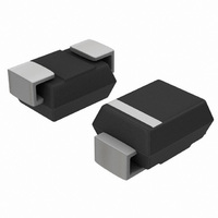
... SCHOTTKY BARRIER RECTIFIER 1.0 AMPERE 90, 100 VOLTS SMB CASE 403A PLASTIC MARKING DIAGRAM AYW B1xG B1 = Device Code for MBRS1100T3 9 for MBRS190T3 A = Assembly Location Y = Year W = Work Week G = Pb−Free Package ORDERING INFORMATION See detailed ordering and shipping information in the package dimensions section on page 2 of this data sheet. ...

Page 2

... Pulse Test: Pulse Width = 300 ms, Duty Cycle ≤ 2.0%. ORDERING INFORMATION Device MBRS1100T3 MBRS1100T3G MBRS190T3 MBRS190T3G †For information on tape and reel specifications, including part orientation and tape sizes, please refer to our Tape and Reel Packaging Specifications Brochure, BRD8011/D. MBRS1100T3, MBRS190T3 Symbol = 25° 1 25° Marking ...

Page 3

... AVERAGE FORWARD CURRENT (AMPS) F(AV) Figure 3. Power Dissipation TYPICAL ELECTRICAL CHARACTERISTICS 280 260 240 220 200 180 160 140 120 100 0.1 0.2 MBRS1100T3, MBRS190T3 1 K 400 200 T = 150°C 100 J 40 125° 100° 0.4 0.2 0.1 0.04 25°C ...

Page 4

... Literature Distribution Center for ON Semiconductor P.O. Box 5163, Denver, Colorado 80217 USA Phone: 303−675−2175 or 800−344−3860 Toll Free USA/Canada Fax: 303−675−2176 or 800−344−3867 Toll Free USA/Canada Email: orderlit@onsemi.com MBRS1100T3, MBRS190T3 PACKAGE DIMENSIONS SMB PLASTIC PACKAGE CASE 403A−03 ...

Related keywords