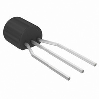
J112RLRAG ON Semiconductor, J112RLRAG Datasheet - Page 2

J112RLRAG
Manufacturer Part Number
J112RLRAG
Description
TRANS GP JFET N-CH 35V TO-92
Manufacturer
ON Semiconductor
Datasheet
1.J112G.pdf
(5 pages)
Specifications of J112RLRAG
Current - Drain (idss) @ Vds (vgs=0)
5mA @ 15V
Fet Type
N-Channel
Voltage - Breakdown (v(br)gss)
35V
Voltage - Cutoff (vgs Off) @ Id
1V @ 1µA
Resistance - Rds(on)
50 Ohm
Mounting Type
Through Hole
Package / Case
TO-92-3 (Standard Body), TO-226
Power - Max
350mW
Configuration
Single
Transistor Polarity
N-Channel
Gate-source Breakdown Voltage
35 V
Drain Current (idss At Vgs=0)
5 mA
Mounting Style
Through Hole
Breakdown Voltage Vbr
35V
Gate-source Cutoff Voltage Vgs(off) Max
-5V
Power Dissipation Pd
350mW
Operating Temperature Range
-65°C To +150°C
No. Of Pins
3
Leaded Process Compatible
Yes
Rohs Compliant
Yes
Lead Free Status / RoHS Status
Lead free / RoHS Compliant
Available stocks
Company
Part Number
Manufacturer
Quantity
Price
Company:
Part Number:
J112RLRAG()
Manufacturer:
MOT
Quantity:
2 059
1. Pulse Width = 300 ms, Duty Cycle = 3.0%.
†For information on tape and reel specifications, including part orientation and tape sizes, please refer to our Tape and Reel Packaging
ELECTRICAL CHARACTERISTICS
OFF CHARACTERISTICS
ON CHARACTERISTICS
ORDERING INFORMATION
Specifications Brochure, BRD8011/D.
Gate −Source Breakdown Voltage
Gate Reverse Current
Gate Source Cutoff Voltage
Drain−Cutoff Current
Zero−Gate−Voltage Drain Current
Static Drain−Source On Resistance
Drain Gate and Source Gate On−Capacitance
Drain Gate Off−Capacitance
Source Gate Off−Capacitance
J111RL1
J111RL1G
J111RLRA
J111RLRAG
J111RLRP
J111RLRPG
J112
J112G
J112RL1
J112RL1G
J112RLRA
J112RLRAG
(I
(V
(V
(V
(V
(V
(V
(V
(V
G
GS
DS
DS
DS
DS
DS
GS
GS
= −1.0 mAdc)
= 5.0 Vdc, I
= 5.0 Vdc, V
= 15 Vdc)
= 0.1 Vdc)
= V
= −15 Vdc)
= −10 Vdc, f = 1.0 MHz)
= −10 Vdc, f = 1.0 MHz)
GS
Device
= 0, f = 1.0 MHz)
D
GS
= 1.0 mAdc)
= −10 Vdc)
Characteristic
(1)
(T
A
= 25°C unless otherwise noted)
http://onsemi.com
J111, J112
(Pb−Free)
(Pb−Free)
(Pb−Free)
(Pb−Free)
(Pb−Free)
(Pb−Free)
Package
TO−92
TO−92
TO−92
TO−92
TO−92
TO−92
TO−92
TO−92
TO−92
TO−92
TO−92
TO−92
2
J112
J112
J112
J111
J111
J111
V
Symbol
V
C
C
r
C
C
(BR)GSS
I
DS(on)
I
GS(off)
I
D(off)
dg(on)
sg(on)
dg(off)
sg(off)
GSS
DSS
+
2000 Units / Tape & Reel
2000 Units / Tape & Reel
2000 Units / Tape & Reel
2000 Units / Tape & Reel
2000 Units / Tape & Reel
−3.0
−1.0
Min
5.0
2.0
35
20
1000 Units / Bulk
−
−
−
−
−
−
−
Shipping
Max
−1.0
−5.0
−10
1.0
5.0
5.0
30
50
28
−
−
−
−
†
mAdc
nAdc
nAdc
Unit
Vdc
Vdc
pF
pF
pF
W


