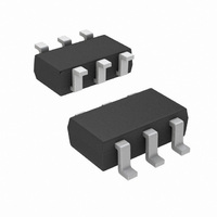
SI3552DV-T1-E3 Vishay, SI3552DV-T1-E3 Datasheet

SI3552DV-T1-E3
Specifications of SI3552DV-T1-E3
Available stocks
Related parts for SI3552DV-T1-E3
SI3552DV-T1-E3 Summary of contents
Page 1
... P Channel P-Channel - 30 30 TSOP-6 Top View 2.85 mm Ordering Information: Si3552DV-T1 ABSOLUTE MAXIMUM RATINGS (T Parameter Drain-Source Voltage Gate-Source Voltage Continuous Drain Current (T Continuous Drain Current (T = 150_C) = 150_C Pulsed Drain Current Continuous Source Current (Diode Conduction Maximum Power Dissipation Maximum Power Dissipation ...
Page 2
... Si3552DV Vishay Siliconix SPECIFICATIONS (T = 25_C UNLESS OTHERWISE NOTED) J Parameter Symbol Static Gate Threshold Voltage Gate Threshold Voltage Gate-Body Leakage Gate Body Leakage Zero Gate Voltage Drain Current Zero Gate Voltage Drain Current a a On-State Drain Current On State Drain Current a a Drain Source On State Resistance ...
Page 3
... I - Drain Current (A) D Gate Charge 1 Total Gate Charge (nC) g Document Number: 70971 S-31725—Rev. B, 18-Aug- Si3552DV Vishay Siliconix NCHANNEL Transfer Characteristics 55_C C 25_C Gate-to-Source Voltage (V) GS Capacitance 300 250 C iss 200 150 100 C oss 50 C rss Drain-to-Source Voltage (V) DS On-Resistance vs ...
Page 4
... Si3552DV Vishay Siliconix TYPICAL CHARACTERISTICS (25_C UNLESS NOTED) Source-Drain Diode Forward Voltage 150_C J 1 0.1 0.00 0.2 0.4 0 Source-to-Drain Voltage (V) SD Threshold Voltage 0 250 mA D 0.2 - 0.0 - 0.2 - 0.4 - 0 Temperature (_C) J Normalized Thermal Transient Impedance, Junction-to-Ambient 2 1 Duty Cycle = 0.5 ...
Page 5
... V 0.2 0.1 0 Drain Current (A) D Document Number: 70971 S-31725—Rev. B, 18-Aug-03 Normalized Thermal Transient Impedance, Junction-to-Foot - Square Wave Pulse Duration (sec Si3552DV Vishay Siliconix NCHANNEL - PCHANNEL Transfer Characteristics 55_C C 6 25_C Gate-to-Source Voltage (V) GS Capacitance 300 240 C iss 180 120 ...
Page 6
... Si3552DV Vishay Siliconix TYPICAL CHARACTERISTICS (25_C UNLESS NOTED) Gate Charge 1 Total Gate Charge (nC) g Source-Drain Diode Forward Voltage 150_C 0.1 0.00 0.3 0.6 0 Source-to-Drain Voltage (V) SD Threshold Voltage 0.6 0.4 0 250 mA D 0.0 - 0 Temperature (_C) J www.vishay.com 25_C 1.2 1.5 100 ...
Page 7
... Single Pulse 0. Document Number: 70971 S-31725—Rev. B, 18-Aug-03 Normalized Thermal Transient Impedance, Junction-to-Ambient - Square Wave Pulse Duration (sec) Normalized Thermal Transient Impedance, Junction-to-Foot - Square Wave Pulse Duration (sec) Si3552DV Vishay Siliconix PCHANNEL Notes Duty Cycle Per Unit Base = R = 130_C/W thJA (t) 3 ...
Page 8
... Vishay disclaims any and all liability arising out of the use or application of any product described herein or of any information provided herein to the maximum extent permitted by law. The product specifications do not expand or otherwise modify Vishay’ ...


