SH8M3TB1 Rohm Semiconductor, SH8M3TB1 Datasheet
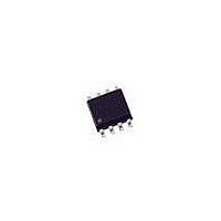
MOSFET N/P-CH 30V SOP8

SH8M3TB1

Manufacturer Part Number
SH8M3TB1
Description
MOSFET N/P-CH 30V SOP8
Manufacturer
Rohm Semiconductor
Datasheet

Specifications of SH8M3TB1

Fet Type
N and P-Channel
Fet Feature
Logic Level Gate
Rds On (max) @ Id, Vgs
51 mOhm @ 5A, 10V
Drain To Source Voltage (vdss)
30V
Current - Continuous Drain (id) @ 25° C
5A, 4.5A
Vgs(th) (max) @ Id
2.5V @ 1mA
Gate Charge (qg) @ Vgs
3.9nC @ 5V
Input Capacitance (ciss) @ Vds
230pF @ 10V
Power - Max
2W
Mounting Type
Surface Mount
Package / Case
8-SOP
Transistor Polarity
N and P-Channel
Resistance Drain-source Rds (on)
58 mOhms
Forward Transconductance Gfs (max / Min)
3 S
Drain-source Breakdown Voltage
30 V
Continuous Drain Current
5 A
Power Dissipation
2 W
Maximum Operating Temperature
+ 150 C
Mounting Style
SMD/SMT
Lead Free Status / RoHS Status
Lead free / RoHS Compliant
Other names
SH8M3TB1TR
4V Drive Nch+Pch MOSFET
Structure
Features
1) Low on-resistance.
2) Built-in G-S Protection Diode.
3) Small Surface Mount Package (SOP8).
Application
Power switching, DC / DC converter.
Packaging specifications
Absolute maximum ratings (Ta=25C)
∗1 Pw≤10μs, Duty cycle≤1%
∗2 MOUNTED ON A CERAMIC BOARD.
Thermal resistance
∗MOUNTED ON A CERAMIC BOARD.
Drain-source voltage
Gate-source voltage
Drain current
Source current
(Body diode)
Total power dissipation
Channel temperature
Storage temperature
Channel to ambient
c
Type
SH8M3
www.rohm.com
Silicon N-channel / P-channel MOSFET
SH8M3
2009 ROHM Co., Ltd. All rights reserved.
Parameter
Parameter
Package
Code
Basic ordering unit (pieces)
Continuous
Pulsed
Continuous
Pulsed
Taping
2500
Rth (ch-a)
TB
Symbol
Symbol
V
V
Tstg
Tch
I
I
P
DSS
GSS
I
I
DP
SP
D
S
D
∗1
∗1
∗2
Nchannel
Limits
±5.0
±20
±20
62.5
1.6
30
20
−55 to +150
Limits
150
2
Pchannel
±4.5
−1.6
−30
±20
±18
−18
°C / W
1/5
Unit
Unit
°C
°C
W
V
V
A
A
A
A
Dimensions (Unit : mm)
Inner circuit
∗A protection diode is included between the gate and
∗2
the source terminals to protect the diode against static
electricity when the product is in use. Use the protection
circuit when the fixed voltages are exceeded.
∗1 ESD PROTECTION DIODE
∗2 BODY DIODE
SOP8
(8)
(1)
∗1
(7)
(2)
∗2
(6)
(3)
∗1
(5)
(4)
Each lead has same dimensions
2009.12 - Rev.A
(1) Tr1 (Nch) Source
(2) Tr1 (Nch) Gate
(3) Tr2 (Pch) Source
(4) Tr2 (Pch) Gate
(5) Tr2 (Pch) Drain
(6) Tr2 (Pch) Drain
(7) Tr1 (Nch) Drain
(8) Tr1 (Nch) Drain
(1) (2) (3) (4)
(8) (7) (6) (5)

Related parts for SH8M3TB1

SH8M3TB1 Summary of contents

Page 1

Drive Nch+Pch MOSFET SH8M3 Structure Silicon N-channel / P-channel MOSFET Features 1) Low on-resistance. 2) Built-in G-S Protection Diode. 3) Small Surface Mount Package (SOP8). Application Power switching converter. Packaging specifications Package Taping Type Code TB ...

Page 2

SH8M3 N-ch Electrical characteristics (Ta=25C) Parameter Symbol Min. Gate-source leakage I GSS Drain-source breakdown voltage V 30 (BR) DSS Zero gate voltage drain current I DSS Gate threshold voltage V 1.0 GS (th) Static drain-source on-state ∗ (on) ...

Page 3

SH8M3 P-ch Electrical characteristics (Ta=25C) Parameter Symbol Min. Gate-source leakage I GSS −30 Drain-source breakdown voltage V (BR) DSS Zero gate voltage drain current I DSS −1.0 Gate threshold voltage V GS (th) Static drain-source on-state ∗ (on) ...

Page 4

SH8M3 N-ch Electrical characteristic curves 1000 Ta=25°C f=1MHz = iss 100 C oss C rss 10 0.01 0 100 DRAIN-SOURCE VOLTAGE : V (V) DS Fig.1 Typical Capacitance vs. Drain-Source Voltage 10 =10V V DS ...

Page 5

SH8M3 P-ch Electrical characteristic curves 10000 Ta=25°C f=1MHz = 1000 C iss C oss 100 C rss 10 0.01 0 100 DRAIN-SOURCE VOLTAGE : −V (V) DS Fig.1 Typical Capacitance vs. Drain-Source Voltage 10 = −10V ...

Page 6

No copying or reproduction of this document, in part or in whole, is permitted without the consent of ROHM Co.,Ltd. The content specified herein is subject to change for improvement without notice. The content specified herein is for the purpose ...

Related keywords