NTHD2102PT1G ON Semiconductor, NTHD2102PT1G Datasheet
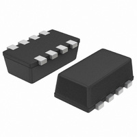
MOSFET PWR P-CH DUAL 8V CHIPFET

NTHD2102PT1G

Manufacturer Part Number
NTHD2102PT1G
Description
MOSFET PWR P-CH DUAL 8V CHIPFET
Manufacturer
ON Semiconductor
Datasheet

Specifications of NTHD2102PT1G

Fet Type
2 P-Channel (Dual)
Fet Feature
Logic Level Gate
Rds On (max) @ Id, Vgs
58 mOhm @ 3.4A, 4.5V
Drain To Source Voltage (vdss)
8V
Current - Continuous Drain (id) @ 25° C
3.4A
Vgs(th) (max) @ Id
1.5V @ 250µA
Gate Charge (qg) @ Vgs
16nC @ 2.5V
Input Capacitance (ciss) @ Vds
715pF @ 6.4V
Power - Max
1.1W
Mounting Type
Surface Mount
Package / Case
8-ChipFET™
Configuration
Dual Dual Drain
Transistor Polarity
P-Channel
Resistance Drain-source Rds (on)
0.058 Ohm @ 4.5 V
Forward Transconductance Gfs (max / Min)
8 S
Drain-source Breakdown Voltage
8 V
Gate-source Breakdown Voltage
+/- 8 V
Continuous Drain Current
3.4 A
Power Dissipation
1100 mW
Maximum Operating Temperature
+ 150 C
Mounting Style
SMD/SMT
Minimum Operating Temperature
- 55 C
Lead Free Status / RoHS Status
Lead free / RoHS Compliant
Other names
NTHD2102PT1GOS
NTHD2102PT1GOS
NTHD2102PT1GOSTR

Available stocks

Company
Part Number
Manufacturer
Quantity
Price
Part Number:
NTHD2102PT1G
Manufacturer:
ON
Quantity:
36 000
Part Number:
NTHD2102PT1G
Manufacturer:
ON/安森美
Quantity:
20 000
NTHD2102P
Power MOSFET
−8.0 V, −4.6 A Dual P−Channel ChipFETt
Features
Applications
Maximum ratings are those values beyond which device damage can occur.
Maximum ratings applied to the device are individual stress limit values (not
normal operating conditions) and are not valid simultaneously. If these limits are
exceeded, device functional operation is not implied, damage may occur and
reliability may be affected.
1. Surface Mounted on FR4 Board using 1 in sq pad size (Cu area = 1.27 in sq
MAXIMUM RATINGS (T
© Semiconductor Components Industries, LLC, 2005
November, 2005 − Rev. 5
Drain−to−Source Voltage
Gate−to−Source Voltage − Continuous
Drain Current − Continuous
Total Power Dissipation
Operating Junction and Storage Temperature
Continuous Source Current
Thermal Resistance (Note 1)
Maximum Lead Temperature for Soldering
making it an Ideal Device for Applications where Board Space is at a
Premium
Environments such as Portable Electronics
Operating Voltage used in many Logic ICs in Portable Electronics
Voltages are not Required
Migration to Lower Levels using the same Basic Topology
Portable Equipment such as MP3 Players, Cell Phones, Digital
Cameras, Personal Digital Assistant and other Portable Applications
Offers an Ultra Low R
Miniature ChipFET Package 40% Smaller Footprint than TSOP−6
Low Profile (<1.1 mm) Allows it to Fit Easily into Extremely Thin
Designed to Provide Low R
Simplifies Circuit Design since Additional Boost Circuits for Gate
Operated at Standard Logic Level Gate Drive, Facilitating Future
Pb−Free Package is Available
Optimized for Battery and Load Management Applications in
Charge Control in Battery Chargers
Buck and Boost Converters
[1 oz] including traces).
Continuous @ T
(5 sec) @ T
Continuous @ 85°C
(5 sec) @ 85°C
Range
(Diode Conduction)
Junction−to−Ambient, 5 sec
Junction−to−Ambient, Continuous
Purposes, 1/8″ from case for 10 seconds
A
− 5 seconds
= 25°C
Rating
A
= 25°C
J
DS(on)
= 25°C unless otherwise noted)
DS(on)
Solution in the ChipFET Package
at Gate Voltage as Low as 1.8 V, the
Symbol
T
V
R
R
J
V
P
, T
T
DSS
I
I
Is
qJA
qJA
GS
D
D
D
L
stg
−55 to
Value
"8.0
+150
−8.0
−3.4
−4.6
−1.1
113
260
1.1
2.1
0.6
1.1
60
1
°C/W
Unit
°C
°C
W
V
V
A
A
G
NTHD2102PT1
NTHD2102PT1G
†For information on tape and reel specifications,
1
P−Channel MOSFET
including part orientation and tape sizes, please
refer to our Tape and Reel Packaging Specifications
Brochure, BRD8011/D.
V
D
D
D
D
−8.0 V
(BR)DSS
CONNECTIONS
1
1
2
2
Device
8
7
6
5
ORDERING INFORMATION
S
PIN
D5 = Specific Device Code
M
G
1
http://onsemi.com
100 mW @ −1.8 V
50 mW @ −4.5 V
68 mW @ −2.5 V
= Month Code
= Pb−Free Package
D
R
1
2
3
4
1
DS(on)
(Pb−Free)
Package
ChipFET
ChipFET
S
G
S
G
1
2
1
2
Publication Order Number:
TYP
G
2
P−Channel MOSFET
1
2
3
4
CASE 1206A
MARKING
DIAGRAM
3000/Tape & Reel
3000/Tape & Reel
ChipFET
STYLE 2
Shipping
NTHD2102P/D
S
I
2
D
−4.6 A
MAX
D
2
8
7
6
5

Related parts for NTHD2102PT1G

NTHD2102PT1G Summary of contents

Page 1

... Is −1.1 A °C qJA R 113 qJA Device °C T 260 L NTHD2102PT1 NTHD2102PT1G †For information on tape and reel specifications, including part orientation and tape sizes, please refer to our Tape and Reel Packaging Specifications Brochure, BRD8011/D. 1 http://onsemi.com R TYP I MAX DS(on −4 −2.5 V −4.6 A 100 mW @ −1.8 V ...

Page 2

ELECTRICAL CHARACTERISTICS Characteristic OFF CHARACTERISTICS Drain−to−Source Breakdown Voltage (Note 2) Temperature Coefficient (Positive) Gate−Body Leakage Current Zero Zero Gate Voltage Drain Current ON CHARACTERISTICS (Note 2) Gate Threshold Voltage Static Drain−to−Source On−Resistance Forward Transconductance Diode Forward Voltage DYNAMIC CHARACTERISTICS Input ...

Page 3

TYPICAL ELECTRICAL CHARACTERISTICS 10 −2.4 thru − −V , Drain−to−Source Voltage (V) DS Figure 1. On−Region Characteristics 0.30 0. −1 0.20 0.15 0.10 0. ...

Page 4

TYPICAL ELECTRICAL CHARACTERISTICS − Total Gate Charge (nC) g, Figure 7. Gate−to−Source and Drain−to−Source Voltage vs. Total Charge ...

Page 5

TYPICAL ELECTRICAL CHARACTERISTICS 2 1 Duty Cycle = 0.5 0.2 0.1 0.1 0.05 0.02 Single Pulse 0.01 −4 − Figure 11. Normalized Thermal Transient Impedance, Junction−to−Ambient 2 1 Duty Cycle = 0.5 0.2 0.1 0.1 0.05 0.02 ...

Page 6

... SCALE 20:1 0.026 Basic *For additional information on our Pb−Free strategy and soldering details, please download the ON Semiconductor Soldering and Mounting Techniques Reference Manual, SOLDERRM/D. ChipFET is a trademark of Vishay Siliconix. ON Semiconductor and are registered trademarks of Semiconductor Components Industries, LLC (SCILLC). SCILLC reserves the right to make changes without further notice to any products herein ...

Related keywords