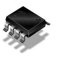
U4083B-MFPG3Y Atmel, U4083B-MFPG3Y Datasheet - Page 3

U4083B-MFPG3Y
Manufacturer Part Number
U4083B-MFPG3Y
Description
Audio Amplifiers COM.CORDED AUDIO AMP
Manufacturer
Atmel
Datasheet
1.U4083B-MFPY_19.pdf
(16 pages)
Specifications of U4083B-MFPG3Y
Product
Class-AB
Output Power
400 mW
Available Set Gain
80 dB
Thd Plus Noise
0.6 %, 0.5 %
Operating Supply Voltage
3 V, 5 V, 9 V
Supply Current
0.065 mA
Maximum Power Dissipation
440 mW
Maximum Operating Temperature
+ 70 C
Mounting Style
SMD/SMT
Audio Load Resistance
100 Ohms
Input Bias Current (max)
0.2 uA
Input Signal Type
Single
Minimum Operating Temperature
- 20 C
Output Signal Type
Differential
Supply Type
Single
Supply Voltage (max)
16 V
Supply Voltage (min)
2 V
Output Type
1-Channel Mono
Package / Case
SOIC-8
Available stocks
Company
Part Number
Manufacturer
Quantity
Price
Part Number:
U4083B-MFPG3Y
Manufacturer:
ATMEL/爱特梅尔
Quantity:
20 000
Part Number:
U4083B-MFPG3Y 19
Manufacturer:
ATMEL/爱特梅尔
Quantity:
20 000
3. Functional Description Including External Circuitry
3.1
3.2
4655C–CORD–03/06
Pin 1: Chip Disable Digital Input (CD)
Pins 2 and 3: Filtering, Power Supply Rejection
Pin 1 (chip disable) is used to power down the IC to conserve power or mute the IC or both.
Input impedance at Pin 1 is typically 90 k .
Figure 8-15 on page 12
from normal operation to muted operation (muting) is more than 70 dB.
Switching characteristics are as follows:
They are independent of C
Voltages at Pins 2 and 3 are supplied from V
is disabled. The outputs, V
removing the signal from the speaker.
When signals are applied from an external source to the outputs (disabled), they must not
exceed the range between the supply voltage, V
Power supply rejection is provided by capacitors C
dominant at high frequencies whereas C
to
For example, a line-powered speakerphone (telephone amplifier) will require more filtering than
a system powered by regulated power supply.
The amount of rejection is a function of the capacitors and the equivalent impedance at Pin 3
and Pin 2 (see electrical characteristic equivalent resistance, R).
Apart from filtering, capacitors C
up, since the capacitors are charged up through the internal resistors (50 k and 125 k ) as
shown in the block diagram.
Figure 8-1 on page 7
The turn-on time is 60% longer when V
The turn-off time is less than 10 µs.
• Logic 0 < 0.8V
• Logic 1 > 2V
• Turn-on time
• Turn-off time
Figure 8-7 on page
IC enabled (normal operation)
IC disabled
shows the turn-on time versus C
9). The values of C
t
t
on
off
shows the power supply current diagram. The change in differential gain
= 12 ms to 15 ms
2 µs
1
, C
O1
2
(Pin 5) and V
and V
1
and C
S
.
S
2
2
= 3V and 20% shorter when V
1
also influence the turn-on time of the circuit at power
is dominant at low frequencies
and C
O2
S
and, therefore, do not change when the U4083B
(Pin 8), turn to a high impedance condition by
S
2
, and ground.
1
depend on the conditions of each application.
and C
2
at V
2
at Pin 3 and Pin 2, respectively. C
S
= 6V, for two different C
S
= 9V.
(Figure 8-4 on page 8
U4083B
1
values.
1
is
3


