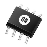
MC100LVEL33DR2 ON Semiconductor, MC100LVEL33DR2 Datasheet - Page 2

MC100LVEL33DR2
Manufacturer Part Number
MC100LVEL33DR2
Description
Clock Drivers & Distribution 3.3V ECL Divide By 4
Manufacturer
ON Semiconductor
Datasheet
1.MC100LVEL33DT.pdf
(8 pages)
Specifications of MC100LVEL33DR2
Mounting Style
SMD/SMT
Package / Case
SOIC-8
Lead Free Status / RoHS Status
Lead free / RoHS Compliant
Available stocks
Company
Part Number
Manufacturer
Quantity
Price
Part Number:
MC100LVEL33DR2
Manufacturer:
ON/安森美
Quantity:
20 000
Part Number:
MC100LVEL33DR2G
Manufacturer:
ON/安森美
Quantity:
20 000
Stresses exceeding Maximum Ratings may damage the device. Maximum Ratings are stress ratings only. Functional operation above the
Recommended Operating Conditions is not implied. Extended exposure to stresses above the Recommended Operating Conditions may affect
device reliability.
1. JEDEC standard multilayer board − 2S2P (2 signal, 2 power)
Table 2. MAXIMUM RATINGS
V
V
V
I
I
T
T
q
q
q
q
q
T
q
Symbol
out
BB
A
stg
JA
JC
JA
JC
JA
sol
JC
CC
EE
I
Figure 1. Logic Diagram and Pinout Assignment
Reset
CLK
CLK
V
BB
PECL Mode Power Supply
NECL Mode Power Supply
PECL Mode Input Voltage
NECL Mode Input Voltage
Output Current
V
Operating Temperature Range
Storage Temperature Range
Thermal Resistance (Junction−to−Ambient)
Thermal Resistance (Junction−to−Case)
Thermal Resistance (Junction−to−Ambient)
Thermal Resistance (Junction−to−Case)
Thermal Resistance (Junction−to−Ambient)
Wave Solder
Thermal Resistance (Junction−to−Case)
BB
1
2
3
4
Sink/Source
Parameter
÷4
R
Pb−Free
8
7
6
5
Pb
V
Q
Q
V
CC
EE
http://onsemi.com
V
V
V
V
Continuous
Surge
0 lfpm
500 lfpm
Standard Board
0 lfpm
500 lfpm
Standard Board
0 lfpm
500 lfpm
<2 to 3 sec @ 248°C
<2 to 3 sec @ 260°C
(Note 1)
EE
CC
EE
CC
Condition 1
= 0 V
= 0 V
= 0 V
= 0 V
2
Table 1. PIN DESCRIPTION
* Pins will default LOW when open due to internal 75 kW
resistor to V
** Pins will default to 1/2 V
resistors: 75 kW to V
CLK*, CLK**
Q, Q
Reset*
V
V
V
PIN
EP
BB
CC
EE
V
V
8 SOIC
8 SOIC
8 SOIC
8 TSSOP
8 TSSOP
8 TSSOP
DFN8
DFN8
DFN8
EE
I
I
V
V
Condition 2
CC
EE
EE
FUNCTION
ECL Differential Clock Inputs
ECL Differential Data ÷4 Outputs
ECL Asynch Reset
Reference Voltage Output
Positive Supply
Negative Supply
(DFN8 only) Thermal Exposed pad
must be connected to a sufficient
thermal conduit. Electrically connect
to the most negative supply (GND)
or leave unconnected, floating open.
and 75 kW to V
CC
when open due to internal
CC
41 to 44 ± 5%
41 to 44 ± 5%
−65 to +150
−40 to +85
35 to 40
Rating
−6 to 0
−8 to 0
8 to 0
6 to 0
± 0.5
100
190
130
185
140
129
265
265
50
84
°C/W
°C/W
°C/W
°C/W
°C/W
°C/W
°C/W
°C/W
°C/W
Unit
mA
mA
mA
°C
°C
°C
V
V
V
V


