MC100EL14DWR2 ON Semiconductor, MC100EL14DWR2 Datasheet
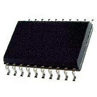
Clock Drivers & Distribution 5V ECL 1:5 Clock

MC100EL14DWR2

Manufacturer Part Number
MC100EL14DWR2
Description
Clock Drivers & Distribution 5V ECL 1:5 Clock
Manufacturer
ON Semiconductor
Datasheet

Specifications of MC100EL14DWR2

Minimum Operating Temperature
- 40 C
Mounting Style
SMD/SMT
Number Of Clock Inputs
2
Output Logic Level
ECL
Supply Voltage (max)
+/- 5.7 V
Supply Voltage (min)
+/- 4.2 V
Maximum Operating Temperature
+ 85 C
Package / Case
SOIC-20 Wide
Lead Free Status / RoHS Status
Lead free / RoHS Compliant
MC100EL14
5V ECL 1:5 Clock
Distribution Chip
explicitly for low skew clock distribution applications. The V
internally generated voltage supply, is available to this device only.
For single-ended input conditions, the unused differential input is
connected to V
rebias AC coupled inputs. When used, decouple V
0.01 mF capacitor and limit current sourcing or sinking to 0.5 mA.
When not used, V
distribution of a lower speed scan or test clock along with the high
speed system clock. When LOW (or left open and pulled LOW by the
input pulldown resistor) the SEL pin will select the differential clock
input.
be enabled/disabled when they are already in the LOW state. This
avoids any chance of generating a runt clock pulse when the device is
enabled/disabled as can happen with an asynchronous control. The
internal flip flop is clocked on the falling edge of the input clock,
therefore all associated specification limits are referenced to the
negative edge of the clock input.
Features
© Semiconductor Components Industries, LLC, 2008
November, 2008 − Rev. 8
The MC100EL14 is a low skew 1:5 clock distribution chip designed
The EL14 features a multiplexed clock input to allow for the
The common enable (EN) is synchronous so that the outputs will only
with V
with V
on Inverted Inputs
50 ps Output-to-Output Skew
Synchronous Enable/Disable
Multiplexed Clock Input
The 100 Series Contains Temperature Compensation
PECL Mode Operating Range: V
NECL Mode Operating Range: V
Q Output will Default LOW with Inputs Open or at V
Internal Input Pull−down Resistors on All Inputs, Pull−up Resistors
EE
EE
= −4.2 V to −5.7 V
= 0 V
BB
BB
as a switching reference voltage. V
should be left open.
CC
CC
= 4.2 V to 5.7 V
= 0 V
BB
and V
BB
EE
BB
may also
CC
1
pin, an
via a
*For additional marking information, refer to
See detailed ordering and shipping information in the package
dimensions section on page 7 of this data sheet.
Application Note AND8002/D.
A
WL
YY
WW
G
ORDERING INFORMATION
20
1
MARKING DIAGRAM
http://onsemi.com
= Assembly Location
= Wafer Lot
= Year
= Work Week
= Pb−Free Package
AWLYYWWG
DW SUFFIX
CASE 751D
SOIC−20L
100EL14
Publication Order Number:
MC100EL14/D

Related parts for MC100EL14DWR2

MC100EL14DWR2 Summary of contents

Page 1

MC100EL14 5V ECL 1:5 Clock Distribution Chip The MC100EL14 is a low skew 1:5 clock distribution chip designed explicitly for low skew clock distribution applications. The V internally generated voltage supply, is available to this device only. For single-ended input ...

Page 2

... Pb−Free Packages are Available* *For additional information on our Pb−Free strategy and soldering details, please download the ON Semiconductor Soldering and Mounting Techniques Reference Manual, SOLDERRM/D. http://onsemi.com 2 ...

Page 3

SCLK CLK CLK All V pins are ...

Page 4

Table 4. MAXIMUM RATINGS Symbol Parameter V PECL Mode Power Supply CC V NECL Mode Power Supply EE V PECL Mode Input Voltage I NECL Mode Input Voltage I Output Current out I V Sink/Source Operating Temperature ...

Page 5

Table 5. 100EL SERIES PECL DC CHARACTERISTICS Symbol Characteristic I Power Supply Current EE V Output HIGH Voltage (Note Output LOW Voltage (Note Input HIGH Voltage (Single−Ended Input LOW Voltage (Single−Ended) IL ...

Page 6

Table 7. AC CHARACTERISTICS V Symbol Characteristic f Maximum Toggle Frequency max (See Figure 2, f /Jitter) MAX t Prop CLK to Q (Diff) PLH t Delay CLK to Q (SE) PHL SCLK Part-to-Part Skew SKEW Within-Device ...

Page 7

... Figure 3. Typical Termination for Output Driver and Device Evaluation (See Application Note AND8020/D − Termination of ECL Logic Devices.) ORDERING INFORMATION4 Device MC100EL14DW MC100EL14DWG MC100EL14DWR2 MC100EL14DWR2G †For information on tape and reel specifications, including part orientation and tape sizes, please refer to our Tape and Reel Packaging Specifications Brochure, BRD8011/ ...

Page 8

Resource Reference of Application Notes AN1405/D − ECL Clock Distribution Techniques AN1406/D − Designing with PECL (ECL at +5.0 V) AN1503/D − ECLinPSt I/O SPiCE Modeling Kit AN1504/D − Metastability and the ECLinPS Family AN1568/D − Interfacing Between LVDS and ...

Page 9

... Equal Opportunity/Affirmative Action Employer. This literature is subject to all applicable copyright laws and is not for resale in any manner. PUBLICATION ORDERING INFORMATION LITERATURE FULFILLMENT: Literature Distribution Center for ON Semiconductor P.O. Box 5163, Denver, Colorado 80217 USA Phone: 303−675−2175 or 800−344−3860 Toll Free USA/Canada Fax: 303− ...

Related keywords