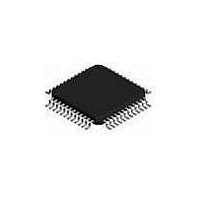
HV461FG-G Supertex, HV461FG-G Datasheet - Page 11

HV461FG-G
Manufacturer Part Number
HV461FG-G
Description
Telephone Ringers Controller IC
Manufacturer
Supertex
Datasheet
1.HV461FG-G.pdf
(14 pages)
Specifications of HV461FG-G
Function
Telecom Ringer
Mounting Style
SMD/SMT
Operating Supply Voltage
4.75 V to 5.25 V
Product
Telecom Ringer
Package / Case
TQFP-48
Frequency
12 Hz, 16.66 Hz, 20 Hz
Maximum Operating Temperature
+ 85 C
Minimum Operating Temperature
- 40 C
Primary Target Application
Generator Circuit
Lead Free Status / RoHS Status
Lead free / RoHS Compliant
Pin Description
Pin
10
11
12
1
2
3
4
5
6
7
8
9
PWMSYNC
DCREF3
CFAULT
PLLFLT
TSYNC
RESET
VREF1
VREF2
FRING
ROSC
AVDD
Name
XTAL
(refer to pin configuration on page 2)
Description
See DCREF1 and DCREF2 (pins 47 & 48).
Outputs a 1.25V nominal reference voltage. Bypass with a 100nF capacitor to ground.
Outputs a 2.50V nominal reference voltage. Bypass with a 100nF capacitor to ground.
Supply for the analog section. 3.0 to 3.6V Must be from the same source as DVDD. Bypass with
a 100nF capacitor to ground as close as possible to the IC.
An RC network connected to this pin determines the SYNC pulse lead time (see SYNC pin 14).
t
A crystal from this pin to ground provides the frequency reference for the internal sine wave
synthesizer. A 19.6608MHz baud rate crystal provides the 8 most common ring frequencies. The
crystal is operated in the series mode. A loading capacitor is not necessary. See also FREQ0–2
(pins 21–23) and FRING (pin 7).
Ring frequency is normally selected from the 8 built-in frequencies using control inputs FREQ0–
2. Other arbitrary frequencies in the range of 12 to 63Hz may be obtained by applying an external
signal to FRING. This external signal sets the ring frequency at a 1:1 ratio. The ring signal
remains a sine wave, with amplitude and offset still controlled via AMPx and OFFx. The ring
signal, while frequency locked to the FRING signal, is not phase–synchronized to it. This allows
the ring signal to immediately start at 0º when enabled via ENABLE or AMP ≠ 00. When unused,
this input must be connected to VGD.
Phase locked loop filter. An RC network connected to this pin stabilizes the PLL that locks on to
the optional external ring frequency signal. (See FRING, pin 7) The RC network determines the
lock time of the PLL. Due to the low frequencies involved, it may take a couple seconds to lock
to the external signal. See the typical application schematic for typical values. When unused, this
pin should be left unconnected.
A resistor from this pin to VDD sets the PWM frequency. f
150kHz)
A capacitor from this pin to ground provides a power–on reset interval. It has an internal 10µA
pull–up to charge the external reset capacitor. Alternatively, an external logic–level or open–
drain signal may be applied to implement the reset function. During the reset interval when
V
time for the host controller to assume control. Use a low leakage tantalum or ceramic capacitor.
t
This pin functions as both an input and an output. It is open–drain with an internal 100µA pull-
up. As an output, it provides a short, low-going pulse at the internal PWM frequency. As an
input, it synchronizes internal PWM frequency to the externally applied signal, provided the
external signal is at a higher frequency. The low-going applied sync pulse should be between
25ns and less than the PWM period in duration. The external source should be open drain. If
the PWMSYNC pins of multiple HV461s are tied together, their PWM frequencies will be phase-
locked to the HV461 with the highest free-running frequency. A maximum of 10 HV461s may be
tied together. If unused, this pin should be left unconnected.
A capacitor from this pin to ground sets the integration time of the FAULT detection circuitry.
A larger capacitor provides less suseptability to transient problems, while a smaller capacitor
provides quicker response. Values in the range of 1µF to 100µF are appropriate. If the FAULT
output is not used, this pin should be grounded. See also FAULT (pin 15).
LEAD
RESET
RESET
= 0.48RC If SYNC is not utilized, TSYNC must still have a connected RC network.
= 1.325V · C
<1.325V, the ringer output is disabled regardless of the state of the ENABLE input, allowing
●
1235 Bordeaux Drive, Sunnyvale, CA 94089
RESET
/ 10µA
11
●
Tel: 408-222-8888
PWM
≈ 12.5GHzΩ / R
●
www.supertex.com
OSC
(valid for 20-
HV461


