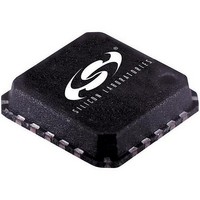
SI5010-BMR Silicon Laboratories Inc, SI5010-BMR Datasheet - Page 11

SI5010-BMR
Manufacturer Part Number
SI5010-BMR
Description
Telecom ICs SONET/SDH 2.5 V OC-3/12 STM-1/4
Manufacturer
Silicon Laboratories Inc
Type
OC-12/3, STM-4/1 Sonet/SDH Clock and Data Recovery Icr
Datasheet
1.SI5010-BM.pdf
(20 pages)
Specifications of SI5010-BMR
Operating Supply Voltage
2.375 V to 2.625 V
Supply Current
124 mA
Operating Temperature Range
- 40 C to + 85 C
Mounting Style
SMD/SMT
Operating Frequency
19.44 MHz
Package / Case
MLP-20
Lead Free Status / RoHS Status
Lead free / RoHS Compliant
4.6. PLL Performance
The PLL implementation used in the Si5010 is fully
compliant with the jitter specifications proposed for
SONET/SDH equipment by Bellcore GR-253-CORE,
Issue 3, September 2000 and ITU-T G.958.
4.6.1. Jitter Tolerance
The Si5010’s tolerance to input jitter exceeds that of the
Bellcore/ITU mask shown in Figure 4. This mask
defines the level of peak-to-peak sinusoid jitter that
must be tolerated when applied to the differential data
input of the device.
4.6.2. Jitter Transfer
The Si5010 is fully compliant with the relevant Bellcore/
ITU specifications related to SONET/SDH jitter transfer.
Jitter transfer is defined as the ratio of output signal jitter
to input signal jitter as a function of jitter frequency (see
Figure 5). These measurements are made with an input
test signal that is degraded with sinusoidal jitter whose
magnitude is defined by the mask in Figure 4.
4.6.3. Jitter Generation
The Si5010 meets all relevant specifications for jitter
generation proposed for SONET/SDH equipment. The
jitter generation specification defines the amount of jitter
that may be present on the recovered clock and data
outputs when a jitter free input signal is provided. The
Si5010 typically generates less than 1.6 mUI
when presented with jitter-free input data.
Jitter (UI p-p)
Figure 4. Jitter Tolerance Specification
Sinusoidal
SONET
Data Rate
OC-12
OC-3
Input
1.5
0.15
15
f0
F0
(Hz)
10
10
f1
F1
(Hz)
30
30
Frequency
f2
F2
(Hz)
300
300
f3
F3
(kHz)
Slope = 20 dB/Decade
6.5
25
ft
Ft
(kHz)
rms
250
65
of jitter
Rev. 1.4
4.7. Powerdown
The Si5010 provides a powerdown pin, PWRDN/CAL,
that disables the device. When the PWRDN/CAL pin is
driven high, the positive and negative terminals of
CLKOUT and DOUT are each tied to VDD through
100 Ω on-chip resistors. This feature is useful in
reducing power consumption in applications that
employ redundant serial channels. When PWRDN/CAL
is released (set to low) the digital logic resets to a
known initial condition, recalibrates the DSPLL
will begin to lock to the data stream.
Note: LOL is not asserted when the device is in the power-
4.8. Device Grounding
The Si5010 uses the GND pad on the bottom of the
20-pin QFN package for device ground. This pad should
be connected directly to the analog supply ground. See
Figures 10 and 11 for the ground (GND) pad location.
4.9. Bias Generation Circuitry
The Si5010 makes use of an external resistor to set
internal bias currents. The external resistor allows
precise generation of bias currents which significantly
reduces
implementations that use an internal resistor. The bias
generation circuitry requires a 10 kΩ (1%) resistor
connected between REXT and GND.
Transfer
Figure 5. Jitter Transfer Specification
0.1 dB
down state.
Jitter
power
Acceptable
consumption
OC-12
OC-3
SONET
Data Rate
Range
Frequency
Fc
Fc
(kHz)
500
130
versus
20 dB/Decade
Si5010
Slope
traditional
®
, and
11


