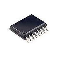
Si3016-KS Silicon Laboratories Inc, Si3016-KS Datasheet - Page 23

Si3016-KS
Manufacturer Part Number
Si3016-KS
Description
Telecom Line Management ICs Line-Side device for processors
Manufacturer
Silicon Laboratories Inc
Type
Chipsetr
Datasheet
1.SI3016-F-FS.pdf
(50 pages)
Specifications of Si3016-KS
Product
Modem Module
Interface Type
Wire
Supply Current
0.3 mA
Maximum Operating Temperature
+ 70 C
Minimum Operating Temperature
0 C
Mounting Style
SMD/SMT
Package / Case
SOIC-16
Lead Free Status / RoHS Status
Lead free / RoHS Compliant
Available stocks
Company
Part Number
Manufacturer
Quantity
Price
Part Number:
SI3016-KS
Manufacturer:
SI
Quantity:
20 000
Part Number:
Si3016-KSR
Manufacturer:
SILICON LABS/芯科
Quantity:
20 000
The receive portion of this mixed signal has a 0 dB gain,
while the transmit signal has a gain of –20 dB.
The transmit and receive signals of the AOUT signal
have independent controls found in Register 6. The
ATM[1:0] bits control the transmit portion, while the
ARM[1:0] bits control the receive portion. The bits only
affect the AOUT signal and do not affect the modem
data. Figure 7 on page 11 illustrates a recommended
application circuit. In the configuration shown, the
LM386 provides a gain of 26 dB. Additional gain
adjustments may be made by varying the voltage
divider created by R1 and R3.
4.21. Gain Control
The Si3016 supports multiple receive gain and transmit
attenuation settings. The receive path can support gains
of 0, 3, 6, 9, and 12 dB, as selected with the ARX[2:0]
bits. The receive path can also be muted with the RXM
bit. The transmit path can support attenuations of 0, 3,
6, 9, and 12 dB, as selected with the ATX[2:0] bits. The
transmit path can also be muted with the TXM bit.
The gain control bits, ARXB and ATXB, should be set to
0 at all times.
4.22. Clocking
The system-side module that the Si3016 connects to is
integrated onto a host processor and is thus clocked
from the processor. The Si3016 receives all clocking
from this system-side module and does not need any
other clock inputs. The sample rate for the Si3016 is
controlled by the Sample Rate Control register.
4.23. Power Management
The Si3016 supports four basic power management
operation modes. The modes are normal operation,
reset operation, sleep mode, and full powerdown mode.
The power management modes are controlled by the
PDN and PDL bits in Register 6.
On powerup or following a reset, the DAA is in reset
operation. In this mode, the PDL bit is set while the PDN
bit is cleared. The system-side module is fully
operational except for the link. No communication
between the system-side module and Si3016 can occur
during reset operation. Note that any register bits
associated with the Si3016 are not valid in this mode.
The most common mode of operation is the normal
operation. In this mode, the PDL and PDN bits are
cleared. The DAA is fully operational, and the link is
passing information between the system-side module
and the Si3016. The desired sample rate should be
programmed prior to entering this mode.
The Si3016 supports a low-power sleep mode. This
Rev. 1.0
mode supports the popular wake-up-on-ring feature of
many modems. To enable it, the PDN bit must be set
and the PDL bit then cleared. When the Si3016 is in
sleep mode, the host processor clock signal may be
stopped or remain active to the system-side module, but
it must be active before waking up the DAA. The
system-side module is non-functional except for the link.
To take the Si3016 out of sleep mode, the system-side
module should be reset.
In summary, the powerdown/up sequence for sleep
mode is as follows:
1. Set the PDN bit and clear the PDL bit.
2. The system-side module clock may stay active or
3. Restore the system-side module clock before
4. Reset the system-side module (after system-side
5. Program registers to desired settings.
The Si3016 also supports an additional power-down
mode. When both the PDN and PDL bits are set, the
chipset enters a complete power-down mode and draws
negligible current (deep sleep mode). In this mode, the
ring detect function does not operate. Normal operation
may be restored using the same process for taking the
DAA out of sleep mode.
4.24. Calibration
The Si3016 initiates an auto-calibration by default
whenever the device goes off-hook or experiences a
loss in line power. Calibration is used to remove any
offsets in the on-chip A/D converter that could affect the
A/D dynamic range. Auto-calibration is typically initiated
after the DAA dc termination stabilizes and takes 512/Fs
seconds to complete. Due to the large variation in line
conditions and line card behavior that can be presented
to the DAA, it may be beneficial to use manual
calibration in lieu of auto-calibration.
Manual calibration should be executed as close to 512/
Fs seconds as possible before valid transmit/receive
data is expected.
The following steps should be taken to implement
manual calibration:
1. The CALD (auto-calibration disable) bit must be set
2. The MCAL (manual calibration) bit must be toggled
3. The calibration will be completed in 512/Fs seconds.
stop.
initiating the powerup sequence.
module clock is present).
to 1.
to one and then zero to begin and complete the
calibration.
Si3016
23


