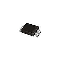
CAT5113YI-10-G ON Semiconductor, CAT5113YI-10-G Datasheet - Page 3

CAT5113YI-10-G
Manufacturer Part Number
CAT5113YI-10-G
Description
Digital Potentiometer ICs DPP,NV 100 taps Up/Down
Manufacturer
ON Semiconductor
Datasheet
1.CAT5113VI-01-G.pdf
(13 pages)
Specifications of CAT5113YI-10-G
Number Of Pots
Single
Taps Per Pot
100
Resistance
10 KOhms
Wiper Memory
Non Volatile
Digital Interface
Serial (3-Wire)
Operating Supply Voltage
3.3 V, 5 V
Supply Current
100 uA
Maximum Operating Temperature
+ 85 C
Minimum Operating Temperature
- 40 C
Mounting Style
SMD/SMT
Supply Voltage (max)
6 V
Supply Voltage (min)
2.5 V
Package / Case
TSSOP-8
Lead Free Status / RoHS Status
Lead free / RoHS Compliant
Available stocks
Company
Part Number
Manufacturer
Quantity
Price
Company:
Part Number:
CAT5113YI-10-GT3
Manufacturer:
XILINX
Quantity:
200
OPERATION MODES
ABSOLUTE MAXIMUM RATINGS
RELIABILITY CHARACTERISTICS
DC ELECTRICAL CHARACTERISTICS
V
Power Supply
Notes:
(1) Stresses above those listed under “Absolute Maximum Ratings” may cause permanent damage to the device. These are stress ratings
(2) This parameter is tested initially and after a design or process change that affects the parameter.
(3) Latch-up protection is provided for stresses up to 100mA on address and data pins from -1V to V
(4) I
(5) These parameters are periodically sampled and are not 100% tested.
© Catalyst Semiconductor, Inc.
Characteristics subject to change without notice
Parameters
Supply Voltage
Inputs
CC
Symbol
Symbol
I
High to Low
High to Low
V
LTH
I
N
SB1
V
I
I
T
only, and functional operation of the device at these or any other conditions outside of those listed in the operational sections of this
specification is not implied. Exposure to any absolute maximum rating for extended periods may affect device performance and reliability.
ZAP
= +2.5V to +6V unless otherwise specified
CC1
CC2
W
END
V
CS
¯¯¯ to GND
INC
U/D ¯ to GND
H to GND
L to GND
W to GND
DR
CC
¯¯ to GND
(2) (3)
High
Low
= source or sink
¯¯¯
INC
(3)
CC
(2)
X
to GND
Parameter
Operating Voltage Range
Supply Current (Increment)
Supply Current (Write)
Supply Current (Standby)
Parameter
ESD Susceptibility
Latch-Up
Data Retention
Endurance
Low to High
Low to High
High
Low
Low
-0.5 to V
-0.5 to V
-0.5 to V
-0.5 to V
-0.5 to V
-0.5 to V
CS
¯¯
-0.5 to +7V
Ratings
CC
CC
CC
CC
CC
CC
High
+0.5
+0.5
+0.5
+0.5
+0.5
+0.5
Low
U/D ¯
X
X
X
Test Method
MIL-STD-883, Test Method 3015
JEDEC Standard 17
MIL-STD-883, Test Method 1008
MIL-STD-883, Test Method 1003
(1)
No Store, Return to Standby
Units
Conditions
V
V
Programming, V
V
CS
U/D ¯ , INC
¯¯ = V
V
V
V
V
V
V
V
CC
CC
CC
Store Wiper Position
= 6V, f = 1MHz, I
= 6V, f = 250kHz, I
= 3V
Wiper toward H
Wiper toward L
¯¯¯ = V
CC
Operation
Standby
- 0.3V
CC
Parameters
Operating Ambient Temperature
Junction Temperature
Storage Temperature
Lead Soldering (10s max)
3
- 0.3V or GND
Commercial (‘C’ or Blank suffix)
Industrial (‘I’ suffix)
CC
= 6V
W
W
= 0
= 0
1,000,000
2000
Min
100
100
Min
2.5
–
–
–
–
–
CC
+ 1V
0.01
Typ
Typ
–
–
–
–
–
-40 to +85
-65 to 150
Ratings
0 to 70
+150
+300
1000
Max
Max
100
500
6.0
50
1
Doc. No. MD-2009 Rev. V
CAT5113
Stores
Years
Units
Units
Units
mA
µA
µA
µA
µA
µA
V
ºC
ºC
ºC
ºC
ºC
V


