IRFR9010 Vishay, IRFR9010 Datasheet

MOSFET P-CH 50V 5.3A DPAK

IRFR9010

Manufacturer Part Number
IRFR9010
Description
MOSFET P-CH 50V 5.3A DPAK
Manufacturer
Vishay
Series
HEXFET®r
Datasheets

Specifications of IRFR9010

Transistor Polarity
P-Channel
Fet Type
MOSFET P-Channel, Metal Oxide
Fet Feature
Standard
Rds On (max) @ Id, Vgs
500 mOhm @ 2.8A, 10V
Drain To Source Voltage (vdss)
50V
Current - Continuous Drain (id) @ 25° C
5.3A
Vgs(th) (max) @ Id
4V @ 250µA
Gate Charge (qg) @ Vgs
9.1nC @ 10V
Input Capacitance (ciss) @ Vds
240pF @ 25V
Power - Max
25W
Mounting Type
Surface Mount
Package / Case
DPak, TO-252 (2 leads+tab), SC-63
Configuration
Single
Drain-source Breakdown Voltage
50 V
Continuous Drain Current
5.3 A
Mounting Style
SMD/SMT
Continuous Drain Current Id
-5.3A
Drain Source Voltage Vds
-50V
On Resistance Rds(on)
350mohm
Rds(on) Test Voltage Vgs
-10V
Threshold Voltage Vgs Typ
-4V
Lead Free Status / RoHS Status
Contains lead / RoHS non-compliant
Other names
*IRFR9010

Available stocks

Company
Part Number
Manufacturer
Quantity
Price
Part Number:
IRFR9010
Manufacturer:
IR
Quantity:
13 600
Part Number:
IRFR9010
Manufacturer:
ST
0
Part Number:
IRFR9010PBF
Manufacturer:
VISHAY
Quantity:
3 398
Part Number:
IRFR9010TR
Manufacturer:
IR
Quantity:
20 000
Part Number:
IRFR9010TRPBF
Manufacturer:
VISHAY
Quantity:
7 938
Note
a. See device orientation.
Notes
a. Repetitive rating; pulse width limited by maximum junction temperature (see fig. 14).
b. V
c. I
d. 0.063" (1.6 mm) from case.
* Pb containing terminations are not RoHS compliant, exemptions may apply
Document Number: 91378
S10-1135-Rev. C, 10-May-10
PRODUCT SUMMARY
V
R
Q
Q
Q
Configuration
ORDERING INFORMATION
Package
Lead (Pb)-free and Halogen-free
Lead (Pb)-free
SnPb
ABSOLUTE MAXIMUM RATINGS T
PARAMETER
Drain-Source Voltage
Gate-Source Voltage
Continuous Drain Current
Pulsed Drain Current
Linear Derating Factor
Single Pulse Avalanche Energy
Repetitive Avalanche Current
Repetitive Avalanche Energy
Maximum Power Dissipation
Peak Diode Recovery dV/dt
Operating Junction and Storage Temperature Range
Soldering Recommendations (Peak Temperature)
(TO-252)
D
DS
DS(on)
g
gs
gd
SD
DPAK
DD
(Max.) (nC)
(nC)
(V)
(nC)
≤ - 5.3 A, dI/dt ≤ - 80 A/μs, V
= - 25 V, starting T
(Ω)
G
S
D
(TO-251)
IPAK
a
J
G
= 25 °C, L = 9.7 mH, R
D S
c
a
a
b
V
GS
DD
= - 10 V
≤ 40 V, T
DPAK (TO-252)
SiHFR9010-GE3
IRFR9010PbF
SiHFR9010-E3
IRFR9010
SiHFR9010
G
Single
P-Channel MOSFET
- 50
IRFR9010, IRFU9010, SiHFR9010, SiHFU9010
9.1
3.0
5.9
J
≤ 150 °C, suggested R
g
C
d
= 25 Ω, peak I
= 25 °C, unless otherwise noted
Power MOSFET
S
D
V
0.50
GS
at - 10 V
T
for 10 s
C
L
DPAK (TO-252)
SiHFR9010TR-GE3
IRFR9010TRPbF
SiHFR9010T-E3
IRFR9010TR
SiHFR9010T
= 25 °C
= - 5.3 A.
T
T
C
g
C
= 100 °C
= 24 Ω.
= 25 °C
FEATURES
• Halogen-free According to IEC 61249-2-21
• Surface Mountable (Order as IRFR9010, SiHFR9010)
• Straight Lead Option (Order as IRFU9010, SiHFU9010)
• Repetitive Avalanche Ratings
• Dynamic dV/dt Rating
• Simple Drive Requirements
• Ease of Paralleling
• Compliant to RoHS Directive 2002/95/EC
DESCRIPTION
The Power MOSFET technology is the key to Vishay’s
advanced line of Power MOSFET transistors. The efficient
geometry and unique processing of this latest “State of the
Art” design achieves: very low on-state resistance
combined with high transconductance; superior reverse
energy and diode recovery dV/dt capability.
The Power MOSFET transistors also feature all of the well
established advantages of MOSFETs such as voltage
control, very fast switching, ease of paralleling and
temperature stability of the electrical parameters.
Surface mount packages enhance circuit performance by
reducing stray inductances and capacitance. The DPAK
(TO-252) surface mount package brings the advantages of
Power MOSFETs to high volume applications where PC
Board surface mounting is desirable. The surface mount
option IRFR9010, SiHFR9010 is provided on 16 mm tape.
The straight lead option IRFU9010, SiHFU9010 of the device
is called the IPAK (TO-251).
They are well suited for applications where limited heat
dissipation is required such as, computers and peripherals,
telecommunication equipment, dc-to-dc converters, and a
wide range of consumer products.
Definition
a
a
a
a
a
SYMBOL
T
dV/dt
J
V
V
E
E
I
I
, T
P
DM
I
AR
GS
DS
AS
AR
D
D
DPAK (TO-252)
SiHFR9010TRL-GE3
IRFR9010TRLPbF
SiHFR9010TL-E3
IRFR9010TRL
SiHFR9010TL
stg
a
a
- 55 to + 150
a
LIMIT
a
± 20
- 5.3
- 3.3
0.20
- 5.3
- 50
- 21
136
300
2.5
5.8
25
a
Vishay Siliconix
IPAK (TO-251)
SiHFU9010-GE3
IRFU9010PbF
SiHFU9010-E3
IRFU9010
SiHFU9010
www.vishay.com
UNIT
W/°C
V/ns
mJ
mJ
°C
V
A
A
W
1

Related parts for IRFR9010

IRFR9010 Summary of contents

Page 1

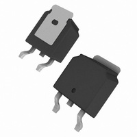
... P-Channel MOSFET Power MOSFETs to high volume applications where PC Board surface mounting is desirable. The surface mount option IRFR9010, SiHFR9010 is provided tape. The straight lead option IRFU9010, SiHFU9010 of the device is called the IPAK (TO-251). They are well suited for applications where limited heat ...

Page 2

... IRFR9010, IRFU9010, SiHFR9010, SiHFU9010 Vishay Siliconix THERMAL RESISTANCE RATINGS PARAMETER Maximum Junction-to-Ambient Case-to-Sink a Maximum Junction-to-Case (Drain) Note a. Mounting pad must cover heatsink surface area. SPECIFICATIONS °C, unless otherwise noted J PARAMETER Static Drain-Source Breakdown Voltage Gate-Source Threshold Voltage Gate-Source Leakage Zero Gate Voltage Drain Current ...

Page 3

... TYPICAL CHARACTERISTICS 25 °C, unless otherwise noted Fig Typical Output Characteristics Fig Typical Transfer Characteristics Fig Typical Saturation Characteristics Document Number: 91378 S10-1135-Rev. C, 10-May-10 IRFR9010, IRFU9010, SiHFR9010, SiHFU9010 Fig Typical Transconductance vs. Drain Current Fig Typical Source-Drain Diode Forward Voltage Vishay Siliconix Fig Maximum Safe Operating Area www.vishay.com ...

Page 4

... IRFR9010, IRFU9010, SiHFR9010, SiHFU9010 Vishay Siliconix Fig Breakdown Voltage vs. Temperature Fig Normalized On-Resistance vs. Temperature www.vishay.com 4 Fig Typical Capacitance vs. Drain-to-Source Voltage Fig Typical Gate Charge vs. Gate-to-Source Voltage Document Number: 91378 S10-1135-Rev. C, 10-May-10 ...

Page 5

... Fig Typical On-Resistance vs. Drain Current Fig Maximum Drain Current vs. Case Temperature Document Number: 91378 S10-1135-Rev. C, 10-May-10 IRFR9010, IRFU9010, SiHFR9010, SiHFU9010 Fig. 13a - Maximum Avalanche vs. Starting Junction Vary t p required I Fig. 13b - Unclamped Inductive Test Circuit Fig. 13c - Unclamped Inductive Waveforms Vishay Siliconix ...

Page 6

... IRFR9010, IRFU9010, SiHFR9010, SiHFU9010 Vishay Siliconix Fig Maximum Effective Transient Thermal Impedance, Junction-to-Case vs. Pulse Duration t t d(on Fig. 15a - Switching Time Waveforms D.U. Pulse width ≤ 1 µs Duty factor ≤ 0.1 % Fig. 15b - Switching Time Test Circuit www.vishay.com d(off Charge Fig. 16a - Basic Gate Charge Waveform Current regulator Same type as D ...

Page 7

... Technology and Package Reliability represent a composite of all qualified locations. For related documents such as package/tape drawings, part marking, and reliability data, see www.vishay.com/ppg?91378. Document Number: 91378 S10-1135-Rev. C, 10-May-10 IRFR9010, IRFU9010, SiHFR9010, SiHFU9010 Peak Diode Recovery dV/dt Test Circuit + Circuit layout considerations • Low stray inductance • ...

Page 8

... Vishay product could result in personal injury or death. Customers using or selling Vishay products not expressly indicated for use in such applications their own risk and agree to fully indemnify and hold Vishay and its distributors harmless from and against any and all claims, liabilities, expenses and damages arising or resulting in connection with such use or sale, including attorneys fees, even if such claim alleges that Vishay or its distributor was negligent regarding the design or manufacture of the part ...

Related keywords