IRFIB7N50A Vishay, IRFIB7N50A Datasheet
IRFIB7N50A
Specifications of IRFIB7N50A
Available stocks


Related parts for IRFIB7N50A

IRFIB7N50A Summary of contents
Page 1
... Soldering Temperature, for 10 seconds Mounting torqe, 6- screw Applicable Off Line SMPS Topologies: Two Transistor Forward l Half & Full Bridge Convertors l Power Factor Correction Boost l Notes through ‡are on page 8 www.irf.com IRFIB7N50A SMPS MOSFET HEXFET V Rds(on) max DSS 500V TO-220 FULLPAK @ 10V GS @ 10V ...
Page 2
... IRFIB7N50A Static @ T = 25°C (unless otherwise specified) J Parameter V Drain-to-Source Breakdown Voltage (BR)DSS Breakdown Voltage Temp. Coefficient (BR)DSS J R Static Drain-to-Source On-Resistance DS(on) V Gate Threshold Voltage GS(th) I Drain-to-Source Leakage Current DSS Gate-to-Source Forward Leakage I GSS Gate-to-Source Reverse Leakage Dynamic @ T = 25°C (unless otherwise specified) ...
Page 3
... BOTTOM 10 ° 100 Fig 2. Typical Output Characteristics 3 2.5 2.0 1.5 1.0 0.5 = 100V 0.0 -60 -40 -20 8.0 9.0 Fig 4. Normalized On-Resistance IRFIB7N50A VGS 15V 10V 8.0V 7.0V 6.0V 5.5V 5.0V 4.5V 20µs PULSE WIDTH 4.5V ° 150 Drain-to-Source Voltage (V) DS 11A V = 10V ...
Page 4
... IRFIB7N50A rss rain-to-S ource V oltage ( Fig 5. Typical Capacitance Vs. Drain-to-Source Voltage 100 10 ° 150 0.1 0.0 0.4 0.8 V ,Source-to-Drain Voltage (V) SD Fig 7. Typical Source-Drain Diode Forward Voltage Fig 6. Typical Gate Charge Vs. 1000 100 10 ° Single Pulse GS 0.1 1.2 1.6 10 Fig 8. Maximum Safe Operating Area 6 ...
Page 5
... Fig 11. Maximum Effective Transient Thermal Impedance, Junction-to-Case www.irf.com R Pulse Width Duty Factor Fig 10a. Switching Time Test Circuit V DS 90% 125 150 ° 10 d(on) Fig 10b. Switching Time Waveforms 1. Duty factor Peak 0.001 0. Rectangular Pulse Duration (sec) 1 IRFIB7N50A D.U. 10V µ d(off ...
Page 6
... IRFIB7N50A Fig 12a. Unclamped Inductive Test Circuit Fig 12b. Unclamped Inductive Waveforms Charge Fig 13a. Basic Gate Charge Waveform Current Regulator Same Type as D.U.T. 50K .2 F 12V .3 F D.U. 3mA Current Sampling Resistors Fig 13b. Gate Charge Test Circuit 6 600 500 ...
Page 7
... Low Leakage Inductance Current Transformer - „ dv/dt controlled Driver same type as D.U.T. I controlled by Duty Factor "D" SD D.U.T. - Device Under Test P.W. Period D = Period Body Diode Forward Current di/dt Diode Recovery dv/dt Body Diode Forward Drop Ripple 5% Fig 14. For N-Channel HEXFETS IRFIB7N50A + =10V ...
Page 8
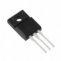
... IRFIB7N50A Package Outline TO-220 Fullpak Outline Dimensions are shown in millimeters (inches (. (. 6.00 (.630) 1 5.80 (.622 3.70 (.540) 1 3.50 (.530) 1 1.0 5 (.04 2) 2.54 (.100 ) 2 X Part Marking Information TO-220 Fullpak Notes: Repetitive rating; pulse width limited by max. junction temperature. ( See fig ‚ ...