IRLR120NPBF International Rectifier, IRLR120NPBF Datasheet - Page 3
IRLR120NPBF
Manufacturer Part Number
IRLR120NPBF
Description
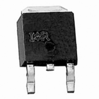
MOSFET N-CH 100V 10A DPAK
Manufacturer
International Rectifier
Series
HEXFET®r
Datasheet
1.IRLR120NTRPBF.pdf
(11 pages)
Specifications of IRLR120NPBF
Fet Type
MOSFET N-Channel, Metal Oxide
Fet Feature
Logic Level Gate
Rds On (max) @ Id, Vgs
185 mOhm @ 6A, 10V
Drain To Source Voltage (vdss)
100V
Current - Continuous Drain (id) @ 25° C
10A
Vgs(th) (max) @ Id
2V @ 250µA
Gate Charge (qg) @ Vgs
20nC @ 5V
Input Capacitance (ciss) @ Vds
440pF @ 25V
Power - Max
48W
Mounting Type
Surface Mount
Package / Case
DPak, TO-252 (2 leads+tab), SC-63
Configuration
Single
Transistor Polarity
N-Channel
Resistance Drain-source Rds (on)
265 mOhms
Drain-source Breakdown Voltage
100 V
Gate-source Breakdown Voltage
16 V
Continuous Drain Current
11 A
Power Dissipation
39 W
Maximum Operating Temperature
+ 175 C
Mounting Style
SMD/SMT
Fall Time
22 ns
Gate Charge Qg
13.3 nC
Minimum Operating Temperature
- 55 C
Rise Time
35 ns
Lead Free Status / RoHS Status
Lead free / RoHS Compliant


and
www.irf.com
100
100
0.1
0.1
10
10
Fig 1. Typical Output Characteristics
Fig 3. Typical Transfer Characteristics
1
1
0.1
2
TOP
BOTTOM 2.5V
V
V
GS
DS
VGS
15V
12V
10V
8.0V
6.0V
4.0V
3.0V
4
, Gate-to-Source Voltage (V)
, Drain-to-Source Voltage (V)
T = 25°C
J
1
6
T = 175°C
2.5V
J
V
20µs PULSE WIDTH
20µs PULSE WIDTH
T = 25°C
DS
J
= 50V
10
8
100
10
A
A
100
0.1
10
3.0
2.5
2.0
1.5
1.0
0.5
0.0
1
0.1
-60 -40 -20
Fig 4. Normalized On-Resistance
Fig 2. Typical Output Characteristics
TOP
BOTTOM 2.5V
I
D
= 10A
V
T , Junction Temperature (°C)
DS
J
VGS
15V
12V
10V
8.0V
6.0V
4.0V
3.0V
Vs. Temperature
IRLR/U120NPbF
, Drain-to-Source Voltage (V)
0
1
20
40
60
20µs PULSE WIDTH
T = 175°C
80 100 120 140 160 180
J
2.5V
10
V
GS
= 10V
3
100
A
A
Related parts for IRLR120NPBF
Image
Part Number
Description
Manufacturer
Datasheet
Request
R

Part Number:
Description:
Advanced Power MOSFET
Manufacturer:
FAIRCHILD [Fairchild Semiconductor]
Datasheet:
Part Number:
Description:
POWER MOSFET
Manufacturer:
IRF [International Rectifier]
Datasheet:
Part Number:
Description:
HEXFET POWER MOSFET
Manufacturer:
IRF [International Rectifier]
Datasheet:
Part Number:
Description:
HEXFET Power MOSFET
Manufacturer:
IRF [International Rectifier]
Datasheet:
Part Number:
Description:
Power MOSFET
Manufacturer:
IRF [International Rectifier]
Datasheet:

Part Number:
Description:
Irlr/u110a Advanced Power Mosfet
Manufacturer:
Fairchild Semiconductor
Datasheet:

Part Number:
Description:
SCHOTTKY RECTIFIER
Manufacturer:
International Rectifier Corp.
Datasheet:
Part Number:
Description:
SCHOTTKY RECTIFIER
Manufacturer:
International Rectifier Corp.
Datasheet:
Part Number:
Description:
SCHOTTKY RECTIFIER
Manufacturer:
International Rectifier Corp.
Datasheet:
Part Number:
Description:
SCHOTTKY RECTIFIER
Manufacturer:
International Rectifier Corp.
Datasheet:
Part Number:
Description:
SCHOTTKY RECTIFIER
Manufacturer:
International Rectifier Corp.
Datasheet:
Part Number:
Description:
SCHOTTKY RECTIFIER
Manufacturer:
International Rectifier Corp.
Datasheet:
Part Number:
Description:
SCHOTTKY RECTIFIER
Manufacturer:
International Rectifier Corp.
Datasheet:
Part Number:
Description:
SCHOTTKY RECTIFIER
Manufacturer:
International Rectifier Corp.
Datasheet:
Part Number:
Description:
SCHOTTKY RECTIFIER
Manufacturer:
International Rectifier Corp.
Datasheet: