IRFB4227PBF International Rectifier, IRFB4227PBF Datasheet
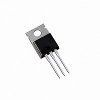
MOSFET N-CH 200V 65A TO-220AB

IRFB4227PBF

Manufacturer Part Number
IRFB4227PBF
Description
MOSFET N-CH 200V 65A TO-220AB
Manufacturer
International Rectifier
Series
HEXFET®r
Type
Power MOSFETr
Datasheets

Specifications of IRFB4227PBF

Fet Type
MOSFET N-Channel, Metal Oxide
Fet Feature
Standard
Rds On (max) @ Id, Vgs
24 mOhm @ 46A, 10V
Drain To Source Voltage (vdss)
200V
Current - Continuous Drain (id) @ 25° C
65A
Vgs(th) (max) @ Id
5V @ 250µA
Gate Charge (qg) @ Vgs
98nC @ 10V
Input Capacitance (ciss) @ Vds
4600pF @ 25V
Power - Max
330W
Mounting Type
Through Hole
Package / Case
TO-220-3 (Straight Leads)
Current, Drain
65 A
Gate Charge, Total
70 nC
Package Type
TO-220AB
Polarization
N-Channel
Power Dissipation
330 W
Resistance, Drain To Source On
19.7 Milliohms
Temperature, Operating, Maximum
+175 °C
Temperature, Operating, Minimum
-40 °C
Time, Turn-off Delay
21 ns
Time, Turn-on Delay
33 ns
Transconductance, Forward
49 S
Voltage, Breakdown, Drain To Source
200 V
Voltage, Forward, Diode
1.3 V
Voltage, Gate To Source
±30 V
Transistor Polarity
N Channel
Continuous Drain Current Id
65A
Drain Source Voltage Vds
200V
On Resistance Rds(on)
19.7mohm
Rds(on) Test Voltage Vgs
10V
Threshold Voltage Vgs Typ
30V
Rohs Compliant
Yes
Drain-source Breakdown Voltage
200 V
Gate-source Breakdown Voltage
30 V
Continuous Drain Current
65 A
Mounting Style
Through Hole
Gate Charge Qg
70 nC
Number Of Elements
1
Polarity
N
Channel Mode
Enhancement
Drain-source On-res
0.024Ohm
Drain-source On-volt
200V
Gate-source Voltage (max)
±30V
Operating Temp Range
-40C to 175C
Operating Temperature Classification
Automotive
Mounting
Through Hole
Pin Count
3 +Tab
Lead Free Status / RoHS Status
Lead free / RoHS Compliant

Available stocks

Company
Part Number
Manufacturer
Quantity
Price
Part Number:
IRFB4227PBF
Manufacturer:
ATHEROS
Quantity:
560
Part Number:
IRFB4227PBF
Manufacturer:
INFINEON/英飞凌
Quantity:
20 000
Part Number:
IRFB4227PBF
0
Company:
Part Number:
IRFB4227PBF
Quantity:
4 800
Company:
Part Number:
IRFB4227PBF
Quantity:
55 200
Description
Notes  through † are on page 8
Features
l
l
l
l
l
l
l
l
l
www.irf.com
Absolute Maximum Ratings
V
I
I
I
I
P
P
T
T
Thermal Resistance
R
R
R
175°C Operating Junction Temperature for
Energy Recovery and Pass Switch Applications
Dissipation in PDP Sustain, Energy Recovery
and Pass Switch Applications
Reliable Operation
Improved Ruggedness
and Reliability
D
D
DM
RP
(Half-bridge)
Advanced Process Technology
Key Parameters Optimized for PDP Sustain,
Low E
Low Q
High Repetitive Peak Current Capability for
Short Fall & Rise Times for Fast Switching
Class-D Audio Amplifier 300W-500W
Repetitive Avalanche Capability for Robustness
J
STG
GS
D
D
θJC
θCS
θJA
@ T
@ T
@T
@T
@ T
HEXFET
C
C
C
C
C
= 25°C
= 100°C
= 25°C
= 100°C
PULSE
G
= 100°C
for Fast Response
MOSFET
®
Rating to Reduce Power
Power MOSFET
Gate-to-Source Voltage
Continuous Drain Current, V
Pulsed Drain Current
Repetitive Peak Current
Power Dissipation
Power Dissipation
Linear Derating Factor
Operating Junction and
Storage Temperature Range
Soldering Temperature for 10 seconds
Mounting Torque, 6-32 or M3 Screw
Junction-to-Case
Case-to-Sink, Flat, Greased Surface
Junction-to-Ambient
f
Parameter
Parameter
f
g
MOSFET
PULSE
GS
GS
@ 10V
@ 10V
V
V
R
I
T
RP
J
DS
DS (Avalanche)
DS(ON)
G
max
max @ T
max
Gate
G
typ. @ 10V
typ.
C
Typ.
0.50
–––
–––
= 100°C
Key Parameters
S
10lb
D
-40 to + 175
IRFB4227PbF
x
in (1.1N
Max.
260
130
330
190
300
±30
2.2
65
46
Drain
D
x
m)
MOSFET
Max.
0.45
–––
62
19.7
200
240
130
175
D
TO-220AB
Source
S
Units
Units
W/°C
°C/W
°C
W
V
A
N
m
°C
G
V
V
A
D
S
1
09/10/07

Related parts for IRFB4227PBF

IRFB4227PBF Summary of contents

Page 1

... Notes  through † are on page 8 www.irf.com V max (Avalanche) R typ. @ 10V DS(ON) I max @ max Gate MOSFET PULSE Parameter @ 10V GS @ 10V GS g Parameter f f IRFB4227PbF Key Parameters 200 typ. 240 m 19.7 = 100°C 130 C 175 TO-220AB D S Drain Source MOSFET Max. Units ± 260 130 330 ...

Page 2

... IRFB4227PbF Electrical Characteristics @ T Parameter BV Drain-to-Source Breakdown Voltage DSS ∆ΒV /∆T Breakdown Voltage Temp. Coefficient DSS J R Static Drain-to-Source On-Resistance DS(on) V Gate Threshold Voltage GS(th) ∆V /∆T Gate Threshold Voltage Coefficient GS(th Drain-to-Source Leakage Current DSS I Gate-to-Source Forward Leakage GSS Gate-to-Source Reverse Leakage ...

Page 3

... V DS, Drain-to -Source Voltage (V) Fig 5. Typical E vs. Drain-to-Source Voltage PULSE www.irf.com 7.0V 10 7.0 8.0 Fig 4. Normalized On-Resistance vs. Temperature 160 170 IRFB4227PbF 1000 VGS TOP 15V 10V 8.0V BOTTOM 7.0V 100 10 ≤ 60µs PULSE WIDTH Tj = 175° Drain-to-Source Voltage (V) Fig 2 ...

Page 4

... IRFB4227PbF 1400 L = 220nH 1200 C= 0.4µF C= 0.3µF 1000 C= 0.2µF 800 600 400 200 100 Temperature (°C) Fig 7. Typical E vs.Temperature PULSE 8000 0V MHZ C iss = SHORTED C rss = oss = 6000 Ciss 4000 Coss 2000 Crss 100 Drain-to-Source Voltage (V) Fig 9. Typical Capacitance vs.Drain-to-Source Voltage ...

Page 5

... Fig 14. Maximum Avalanche Energy Vs. Temperature τ J τ J τ 1 τ 1 Ci= τi/Ri Ci i/Ri 0.0001 0.001 Rectangular Pulse Duration (sec) IRFB4227PbF 600 TOP 500 BOTTOM 400 300 200 100 100 125 Starting Junction Temperature (°C) 200 ton= 1µs Duty cycle = 0.25 Half Sine Wave ...

Page 6

... IRFB4227PbF D.U.T + ƒ • • - • + ‚ -  • • • SD • Fig 18 D.U 20V V GS 0.01 Ω Fig 19a. Unclamped Inductive Test Circuit ≤ 1 ≤ 0.1 % Fig 20a. Switching Time Test Circuit DUT Fig 21a. Gate Charge Test Circuit 6 Driver Gate Drive P ...

Page 7

... Fig 21a. t and E Test Circuit st PULSE Fig 21c. E www.irf.com Fig 21b. t Test Waveforms PULSE IRFB4227PbF Test Waveforms st 7 ...

Page 8

... IRFB4227PbF TO-220AB packages are not recommended for Surface Mount Application. Notes:  Repetitive rating; pulse width limited by max. junction temperature. ‚ Starting T = 25° 0.18mH 25Ω ƒ Pulse width ≤ 400µs; duty cycle ≤ 2%. „ approximately 90° measured at θ J … ...

Related keywords