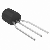
BS107ARL1G ON Semiconductor, BS107ARL1G Datasheet - Page 2

BS107ARL1G
Manufacturer Part Number
BS107ARL1G
Description
MOSFET N-CH 200V 250MA TO-92
Manufacturer
ON Semiconductor
Datasheet
1.BS107ARL1G.pdf
(4 pages)
Specifications of BS107ARL1G
Fet Type
MOSFET N-Channel, Metal Oxide
Fet Feature
Logic Level Gate
Rds On (max) @ Id, Vgs
6.4 Ohm @ 250mA, 10V
Drain To Source Voltage (vdss)
200V
Current - Continuous Drain (id) @ 25° C
250mA
Vgs(th) (max) @ Id
3V @ 1mA
Input Capacitance (ciss) @ Vds
60pF @ 25V
Power - Max
350mW
Mounting Type
Through Hole
Package / Case
TO-92-3 (Standard Body), TO-226
Lead Free Status / RoHS Status
Lead free / RoHS Compliant
Gate Charge (qg) @ Vgs
-
Other names
BS107ARL1GOSTR
Available stocks
Company
Part Number
Manufacturer
Quantity
Price
Company:
Part Number:
BS107ARL1G
Manufacturer:
MICROCHIP
Quantity:
1 001
Part Number:
BS107ARL1G
Manufacturer:
ON/安森美
Quantity:
20 000
3. Pulse Test: Pulse Width v 300 ms, Duty Cycle v 2.0%.
PULSE GENERATOR
ELECTRICAL CHARACTERISTICS
OFF CHARACTERISTICS
ON CHARACTERISTICS (Note 3)
SMALL-SIGNAL CHARACTERISTICS
SWITCHING CHARACTERISTICS
Zero-Gate-Voltage Drain Current (V
Drain-Source Breakdown Voltage (V
Gate Reverse Current (V
Gate Threshold Voltage (I
Static Drain-Source On Resistance
Input Capacitance
Reverse Transfer Capacitance
Output Capacitance
Forward Transconductance
Turn-On Time
Turn-Off Time
BS107 (V
BS107A (V
(V
(V
(V
(V
DS
DS
DS
DS
50
= 25 Vdc, V
= 25 Vdc, V
= 25 Vdc, V
= 25 Vdc, I
(V
(I
(I
D
D
GS
GS
GS
= 100 mAdc)
= 250 mAdc)
= 2.6 Vdc, I
= 10 Vdc, I
= 10 Vdc)
D
GS
GS
GS
= 250 mAdc)
Figure 1. Switching Test Circuit
= 0, f = 1.0 MHz)
= 0, f = 1.0 MHz)
= 0, f = 1.0 MHz)
V
in
GS
50
D
40 pF
= 1.0 mAdc, V
D
= 15 Vdc, V
D
Characteristic
= 200 mAdc)
= 20 mAdc)
1 M
DS
+25 V
GS
= 130 Vdc, V
= 0, I
DS
23
(T
DS
A
= 0)
= 25°C unless otherwise noted)
D
= V
= 100 mAdc)
ATTENUATOR
GS
20 dB
)
50 W
GS
RESISTIVE SWITCHING
BS107, BS107A
= 0)
http://onsemi.com
2
TO SAMPLING SCOPE
50 W INPUT
V
Symbol
V
r
(BR)DSX
DS(on)
I
GS(Th)
C
I
V
C
C
DSS
GSS
g
t
t
out
oss
on
off
rss
OUTPUT V
INVERTED
INPUT V
iss
fs
in
Figure 2. Switching Waveforms
out
10 V
Min
200
200
1.0
-
-
-
-
-
-
-
-
-
-
-
10%
t
on
50%
0.01
Typ
400
4.5
4.8
6.0
6.0
60
30
12
-
-
-
-
-
PULSE WIDTH
90%
Max
3.0
6.0
6.4
30
10
28
14
15
15
90%
-
-
-
-
-
50%
10%
mmhos
t
off
nAdc
nAdc
Unit
90%
Vdc
Vdc
pF
pF
pF
ns
ns
W


