IRL2203S Vishay, IRL2203S Datasheet - Page 2
IRL2203S
Manufacturer Part Number
IRL2203S
Description
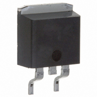
MOSFET N-CH 30V 100A D2PAK
Manufacturer
Vishay
Series
HEXFET®r
Datasheet
1.IRL2203S.pdf
(9 pages)
Specifications of IRL2203S
Fet Type
MOSFET N-Channel, Metal Oxide
Fet Feature
Logic Level Gate
Rds On (max) @ Id, Vgs
7 mOhm @ 60A, 10V
Drain To Source Voltage (vdss)
30V
Current - Continuous Drain (id) @ 25° C
100A
Vgs(th) (max) @ Id
2.5V @ 250µA
Gate Charge (qg) @ Vgs
110nC @ 4.5V
Input Capacitance (ciss) @ Vds
3500pF @ 25V
Power - Max
3.8W
Mounting Type
Surface Mount
Package / Case
D²Pak, TO-263 (2 leads + tab)
Lead Free Status / RoHS Status
Contains lead / RoHS non-compliant
Available stocks
Company
Part Number
Manufacturer
Quantity
Price
Company:

Part Number:
IRL2203S
Manufacturer:
IR
Quantity:
6 800
Company:
Part Number:
IRL2203S
Manufacturer:
IR
Quantity:
12 500


Electrical Characteristics @ T
** When mounted on FR-4 board using minimum recommended footprint.
Source-Drain Ratings and Characteristics
Notes:
R
L
V
V
g
Q
Q
Q
t
t
t
t
C
C
C
I
I
V
t
Q
I
I
DSS
r
SM
d(on)
d(off)
f
S
rr
GSS
S
V
For recommended footprint and soldering techniques refer to application note #AN-994.
fs
DS(on)
(BR)DSS
GS(th)
SD
iss
oss
rss
R
g
gs
gd
rr
Repetitive rating; pulse width limited by
V
(BR)DSS
max. junction temperature. ( See fig. 11 )
I
T
SD
DD
G
J
= 25 , I
= 15V, starting T
175°C
60A, di/dt 140A/µs, V
/ T
J
AS
Static Drain-to-Source On-Resistance
Internal Source Inductance
Drain-to-Source Breakdown Voltage
Breakdown Voltage Temp. Coefficient
Gate Threshold Voltage
Forward Transconductance
Drain-to-Source Leakage Current
Gate-to-Source Forward Leakage
Gate-to-Source Reverse Leakage
Total Gate Charge
Gate-to-Source Charge
Gate-to-Drain ("Miller") Charge
Turn-On Delay Time
Rise Time
Turn-Off Delay Time
Fall Time
Input Capacitance
Output Capacitance
Reverse Transfer Capacitance
Continuous Source Current
(Body Diode)
Pulsed Source Current
(Body Diode)
Diode Forward Voltage
Reverse Recovery Time
Reverse RecoveryCharge
= 60A. (See Figure 12)
J
= 25°C, L = 220µH
Parameter
Parameter
DD
V
(BR)DSS
J
,
= 25°C (unless otherwise specified)
–––
–––
–––
–––
–––
–––
–––
–––
–––
–––
–––
–––
–––
–––
–––
–––
–––
Min. Typ. Max. Units
–––
Min. Typ. Max. Units
1.0
30
–––
–––
–––
47
–––
–––
Pulse width
Calculated continuous current based on maximum allowable
Uses IRL2203N data and test conditions.
package refer to Design Tip # 93-4
junction temperature; for recommended current-handling of the
0.035 –––
3500 –––
1400 –––
7.5
–––
–––
–––
–––
–––
––– -100
–––
–––
690
–––
–––
––– 0.007
–––
–––
–––
210
–––
280
15
29
54
94
100
0.01
–––
–––
100
–––
250
110
–––
–––
–––
–––
–––
400
140
410
2.5
1.3
25
31
57
300µs; duty cycle
V/°C
µA
nA
nC
nH
nC
pF
ns
ns
A
V
V
S
V
V
V
V
V
V
V
ƒ = 1.0MHz, See Fig. 5
Reference to 25°C, I
V
V
V
V
V
V
I
I
R
R
Between lead,
and center of die contact
V
V
MOSFET symbol
showing the
p-n junction diode.
T
T
di/dt = 100A/µs
integral reverse
D
D
J
J
GS
GS
GS
DS
DS
DS
DS
GS
GS
DS
GS
DD
GS
DS
G
D
= 60A
= 60A
= 25°C, I
= 25°C, I
= 1.8
= 0.25
= 10V, I
= 4.5V, I
= 25V, I
= 0V, I
= V
= 30V, V
= 24V, V
= 20V
= -20V
= 24V
= 4.5V, See Fig. 6 and 13
= 15V
= 0V
= 25V
2%.
GS
, I
D
V
S
F
D
D
D
GS
D
See Fig. 10
Conditions
= 60A
= 250µA
= 60A, V
GS
GS
Conditions
= 60A
= 60A
= 250µA
= 50A
= 4.5V
= 0V
= 0V, T
D
GS
= 1mA
J
= 0V
= 150°C
G
D
S
Related parts for IRL2203S
Image
Part Number
Description
Manufacturer
Datasheet
Request
R

Part Number:
Description:
357-036-542-201 CARDEDGE 36POS DL .156 BLK LOPRO
Manufacturer:
Vishay
Datasheet:
Part Number:
Description:
357-036-542-201 CARDEDGE 36POS DL .156 BLK LOPRO
Manufacturer:
Vishay
Datasheet:
Part Number:
Description:
357-036-542-201 CARDEDGE 36POS DL .156 BLK LOPRO
Manufacturer:
Vishay
Datasheet:
Part Number:
Description:
357-036-542-201 CARDEDGE 36POS DL .156 BLK LOPRO
Manufacturer:
Vishay
Datasheet:
Part Number:
Description:
357-036-542-201 CARDEDGE 36POS DL .156 BLK LOPRO
Manufacturer:
Vishay
Datasheet:
Part Number:
Description:
357-036-542-201 CARDEDGE 36POS DL .156 BLK LOPRO
Manufacturer:
Vishay
Datasheet:
Part Number:
Description:
357-036-542-201 CARDEDGE 36POS DL .156 BLK LOPRO
Manufacturer:
Vishay
Datasheet:
Part Number:
Description:
357-036-542-201 CARDEDGE 36POS DL .156 BLK LOPRO
Manufacturer:
Vishay
Datasheet:
Part Number:
Description:
357-036-542-201 CARDEDGE 36POS DL .156 BLK LOPRO
Manufacturer:
Vishay
Datasheet:
Part Number:
Description:
357-036-542-201 CARDEDGE 36POS DL .156 BLK LOPRO
Manufacturer:
Vishay
Datasheet:
Part Number:
Description:
357-036-542-201 CARDEDGE 36POS DL .156 BLK LOPRO
Manufacturer:
Vishay
Datasheet:
Part Number:
Description:
357-036-542-201 CARDEDGE 36POS DL .156 BLK LOPRO
Manufacturer:
Vishay
Datasheet:
Part Number:
Description:
357-036-542-201 CARDEDGE 36POS DL .156 BLK LOPRO
Manufacturer:
Vishay
Datasheet:
Part Number:
Description:
357-036-542-201 CARDEDGE 36POS DL .156 BLK LOPRO
Manufacturer:
Vishay
Datasheet:
Part Number:
Description:
357-036-542-201 CARDEDGE 36POS DL .156 BLK LOPRO
Manufacturer:
Vishay
Datasheet: