IRFP344PBF Vishay, IRFP344PBF Datasheet

MOSFET N-CH 450V 9.5A TO-247AC

IRFP344PBF

Manufacturer Part Number
IRFP344PBF
Description
MOSFET N-CH 450V 9.5A TO-247AC
Manufacturer
Vishay
Datasheet

Specifications of IRFP344PBF

Fet Type
MOSFET N-Channel, Metal Oxide
Fet Feature
Standard
Rds On (max) @ Id, Vgs
630 mOhm @ 5.7A, 10V
Drain To Source Voltage (vdss)
450V
Current - Continuous Drain (id) @ 25° C
9.5A
Vgs(th) (max) @ Id
4V @ 250µA
Gate Charge (qg) @ Vgs
80nC @ 10V
Input Capacitance (ciss) @ Vds
1400pF @ 25V
Power - Max
150W
Mounting Type
Through Hole
Package / Case
TO-247-3 (Straight Leads), TO-247AC
Transistor Polarity
N Channel
Continuous Drain Current Id
9.5A
Drain Source Voltage Vds
450V
On Resistance Rds(on)
630mohm
Rds(on) Test Voltage Vgs
10V
Power Dissipation Pd
150W
Lead Free Status / RoHS Status
Lead free / RoHS Compliant
Other names
*IRFP344PBF

Available stocks

Company
Part Number
Manufacturer
Quantity
Price
Part Number:
IRFP344PBF
Manufacturer:
VISHAY/威世
Quantity:
20 000
Notes
a. Repetitive rating; pulse width limited by maximum junction temperature (see fig. 11).
b. V
c. I
d. 1.6 mm from case.
Document Number: 91223
S09-0006-Rev. A, 19-Jan-09
PRODUCT SUMMARY
V
R
Q
Q
Q
Configuration
ORDERING INFORMATION
Package
Lead (Pb)-free
ABSOLUTE MAXIMUM RATINGS T
PARAMETER
Drain-Source Voltage
Gate-Source Voltage
Continuous Drain Current
Pulsed Drain Current
Linear Derating Factor
Single Pulse Avalanche Energy
Repetitive Avalanche Current
Repetitive Avalanche Energy
Maximum Power Dissipation
Peak Diode Recovery dV/dt
Operating Junction and Storage Temperature Range
Soldering Recommendations (Peak Temperature)
Mounting Torque
DS
DS(on)
g
gs
gd
SD
DD
(Max.) (nC)
(nC)
(nC)
(V)
≤ 9.5 A, dI/dt ≤ 90 A/µs, V
= 50 V, starting T
(Ω)
TO-247
a
G
J
D
= 25 °C, L = 8.1 mH, R
S
c
a
a
DD
b
V
GS
≤ V
= 10 V
DS
G
, T
N-Channel MOSFET
J
Single
≤ 150 °C.
450
80
12
41
G
= 25 Ω, I
D
S
C
Power MOSFET
0.63
= 25 °C, unless otherwise noted
V
GS
AS
6-32 or M3 screw
at 10 V
= 9.5 A (see fig. 12).
T
C
for 10 s
= 25 °C
T
T
C
C
TO-247
IRFP344PbF
SiHFP344-E3
= 100 °C
= 25 °C
FEATURES
• Dynamic dV/dt Rating
• Repetitive Avalanche Rated
• Isolated Central Mounting Hole
• Fast Switching
• Ease of Paralleling
• Simple Drive Requirements
• Lead (Pb)-free
DESCRIPTION
Third generation Power MOSFETs from Vishay provide the
designer with the best combination of fast switching,
ruggedized
cost-effectiveness.
The TO-247 package is preferred for commercial-industrial
applications where higher power levels preclude the use of
TO-220 devices. The TO-247 is similar but superior to the
earlier TO-218 package because its isolated mounting hole.
It also provides greater creepage distances between pins to
meet the requirements of most safety specifications.
SYMBOL
T
dV/dt
J
V
V
E
E
I
I
P
, T
device
I
DM
AR
DS
GS
AS
AR
D
D
stg
IRFP344, SiHFP344
design,
- 55 to + 150
LIMIT
300
± 20
450
410
150
9.5
6.0
1.2
9.5
3.5
1.1
38
15
10
low
d
Vishay Siliconix
on-resistance
www.vishay.com
lbf · in
UNIT
W/°C
N · m
V/ns
mJ
mJ
°C
W
RoHS
V
A
A
COMPLIANT
and
1

Related parts for IRFP344PBF

IRFP344PBF Summary of contents

Page 1

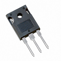
... S TO-220 devices. The TO-247 is similar but superior to the earlier TO-218 package because its isolated mounting hole. N-Channel MOSFET It also provides greater creepage distances between pins to meet the requirements of most safety specifications. TO-247 IRFP344PbF SiHFP344- °C, unless otherwise noted ° ...

Page 2

... IRFP344, SiHFP344 Vishay Siliconix THERMAL RESISTANCE RATINGS PARAMETER Maximum Junction-to-Ambient Case-to-Sink, Flat, Greased Surface Maximum Junction-to-Case (Drain) SPECIFICATIONS °C, unless otherwise noted J PARAMETER Static Drain-Source Breakdown Voltage V Temperature Coefficient DS Gate-Source Threshold Voltage Gate-Source Leakage Zero Gate Voltage Drain Current Drain-Source On-State Resistance ...

Page 3

... TYPICAL CHARACTERISTICS 25 °C, unless otherwise noted Fig Typical Output Characteristics, T Fig Typical Output Characteristics, T Document Number: 91223 S09-0006-Rev. A, 19-Jan- °C Fig Typical Transfer Characteristics C Fig Normalized On-Resistance vs. Temperature = 150 °C C IRFP344, SiHFP344 Vishay Siliconix www.vishay.com 3 ...

Page 4

... IRFP344, SiHFP344 Vishay Siliconix Fig Typical Capacitance vs. Drain-to-Source Voltage Fig Typical Gate Charge vs. Gate-to-Source Voltage www.vishay.com 4 Fig Typical Source-Drain Diode Forward Voltage Fig Maximum Safe Operating Area Document Number: 91223 S09-0006-Rev. A, 19-Jan-09 ...

Page 5

... Fig Maximum Drain Current vs. Case Temperature Fig Maximum Effective Transient Thermal Impedance, Junction-to-Case Document Number: 91223 S09-0006-Rev. A, 19-Jan-09 IRFP344, SiHFP344 Vishay Siliconix D.U. Pulse width ≤ 1 µs Duty factor ≤ 0.1 % Fig. 10a - Switching Time Test Circuit d(on) r d(off) f Fig. 10b - Switching Time Waveforms www ...

Page 6

... IRFP344, SiHFP344 Vishay Siliconix Vary t to obtain p required I AS D.U. 0.01 Ω Fig. 12a - Unclamped Inductive Test Circuit Fig. 12c - Maximum Avalanche Energy vs. Drain Current Charge Fig. 13a - Basic Gate Charge Waveform www.vishay.com Fig. 12b - Unclamped Inductive Waveforms Current regulator Same type as D.U.T. ...

Page 7

... V GS Vishay Siliconix maintains worldwide manufacturing capability. Products may be manufactured at one of several qualified locations. Reliability data for Silicon Technology and Package Reliability represent a composite of all qualified locations. For related documents such as package/tape drawings, part marking, and reliability data, see www.vishay.com/ppg?91223. Document Number: 91223 S09-0006-Rev ...

Page 8

... Vishay disclaims any and all liability arising out of the use or application of any product described herein or of any information provided herein to the maximum extent permitted by law. The product specifications do not expand or otherwise modify Vishay’ ...

Related keywords