IRFP140N International Rectifier, IRFP140N Datasheet
IRFP140N
Specifications of IRFP140N
Available stocks


Related parts for IRFP140N

IRFP140N Summary of contents
Page 1
... Case-to-Sink, Flat, Greased Surface CS R Junction-to-Ambient JA www.irf.com G @ 10V GS @ 10V GS 300 (1.6mm from case) 10 lbf•in (1.1N•m) Min. –––– –––– –––– 91343B IRFP140N 100V DSS R = 0.052 DS(on 33A D S TO-247AC Max. Units ...
Page 2
... IRFP140N Electrical Characteristics @ T Parameter V Drain-to-Source Breakdown Voltage (BR)DSS Breakdown Voltage Temp. Coefficient (BR)DSS J R Static Drain-to-Source On-Resistance DS(on) V Gate Threshold Voltage GS(th) g Forward Transconductance fs I Drain-to-Source Leakage Current DSS Gate-to-Source Forward Leakage I GSS Gate-to-Source Reverse Leakage Q Total Gate Charge g Q Gate-to-Source Charge ...
Page 3
... D rain-to-S ourc e Voltage ( Fig 1. Typical Output Characteristics ° ° 0µ ate-to -So urce Voltag e ( Fig 3. Typical Transfer Characteristics www.irf.com IRFP140N VGS TOP 15V 10V 8.0V 7.0V 6.0V 5.5V 5.0V BOTTOM 4. 4 0µ 5° 0 rain-to-S ource V oltage ( Fig 2. Typical Output Characteristics 3 2.5 2 ...
Page 4
... IRFP140N iss iss oss rss rain-to-S ourc e V oltage ( Fig 5. Typical Capacitance Vs. Drain-to-Source Voltage ° 5° 0.4 0.8 1 ourc e-to-D rain V oltage ( Fig 7. Typical Source-Drain Diode Forward Voltage 1.6 2 FIG otal G ate C harge ( Fig 6. Typical Gate Charge Vs. Gate-to-Source Voltage ITE µ µ ...
Page 5
... Fig 11. Maximum Effective Transient Thermal Impedance, Junction-to-Case www.irf.com R Pulse Width Duty Factor Fig 10a. Switching Time Test Circuit V DS 90% 150 175 10% ° Fig 10b. Switching Time Waveforms Notes: 1. Duty factor Peak 0.001 0. Rectangular Pulse Duration (sec) 1 IRFP140N D.U. 10V µ d(on) r d(off) f ...
Page 6
... IRFP140N V DS D.U. Fig 12a. Unclamped Inductive Test Circuit Fig 12b. Unclamped Inductive Waveforms Charge Fig 13a. Basic Gate Charge Waveform 0. (BR)DSS TTO tarting unc tion T em perature (° Fig 12c. Maximum Avalanche Energy Vs. Drain Current Current Regulator Same Type as D.U.T. ...
Page 7
... Low Leakage Inductance Current Transformer - - dv/dt controlled Driver same type as D.U.T. I controlled by Duty Factor "D" SD D.U.T. - Device Under Test Period D = Period Waveform Body Diode Forward Current di/dt Waveform DS Diode Recovery dv/dt Body Diode Forward Drop Ripple 5% Fig 14. For N-Channel HEXFETS IRFP140N + + P.W. V =10V * ...
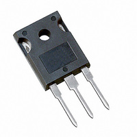
Page 8
... IRFP140N Package Outline TO-247AC Outline Dimensions are shown in millimeters (inches) 1 5.90 (. 5.30 (. .30 (.800) 19 .70 (.775 14.8 0 (.5 83) 14.2 0 (.5 59) 2.40 (.09 4) 2.00 (. 5.45 (.2 15) 3 .40 (.133 ) 2X 3 .00 (.118 ) Part Marking Information TO-247AC WORLD HEADQUARTERS: 233 Kansas St., El Segundo, California 90245, Tel: (310) 322 3331 IR FAR EAST: K& ...
Page 9
Note: For the most current drawings please refer to the IR website at: http://www.irf.com/package/ ...