MTY100N10E ON Semiconductor, MTY100N10E Datasheet

MOSFET N-CH 100V 100A TO-264

MTY100N10E

Manufacturer Part Number
MTY100N10E
Description
MOSFET N-CH 100V 100A TO-264
Manufacturer
ON Semiconductor
Datasheet

Specifications of MTY100N10E

Fet Type
MOSFET N-Channel, Metal Oxide
Fet Feature
Standard
Rds On (max) @ Id, Vgs
11 mOhm @ 50A, 10V
Drain To Source Voltage (vdss)
100V
Current - Continuous Drain (id) @ 25° C
100A
Vgs(th) (max) @ Id
4V @ 250µA
Gate Charge (qg) @ Vgs
378nC @ 10V
Input Capacitance (ciss) @ Vds
10640pF @ 25V
Power - Max
300W
Mounting Type
Through Hole
Package / Case
TO-264-3, TO-3BPL
Lead Free Status / RoHS Status
Contains lead / RoHS non-compliant
Other names
MTY100N10EOS

Available stocks

Company
Part Number
Manufacturer
Quantity
Price
Part Number:
MTY100N10E
Manufacturer:
ON
Quantity:
5 510
Part Number:
MTY100N10E
Manufacturer:
AVAGO
Quantity:
5 510
Company:
Part Number:
MTY100N10E
Quantity:
45
MTY100N10E
Power MOSFET
100 Amps, 100 Volts
N−Channel TO−264
energy in the avalanche and commutation modes. This new energy
efficient design also offers a drain−to−source diode with fast recovery
time. Designed for high voltage, high speed switching applications in
power supplies, converters, PWM motor controls, and other inductive
loads. The avalanche energy capability is specified to eliminate the
guesswork in designs where inductive loads are switched and offer
additional safety margin against unexpected voltage transients.
© Semiconductor Components Industries, LLC, 2006
August, 2006 − Rev. 4
MAXIMUM RATINGS
Drain−Source Voltage
Drain−Gate Voltage (R
Gate−Source Voltage
Drain Current − Continuous @ T
Drain Current
Total Power Dissipation
Operating and Storage Temperature Range
Single Pulse Drain−to−Source Avalanche
Thermal Resistance − Junction to Case
Thermal Resistance
Maximum Lead Temperature for Soldering
This advanced Power MOSFET is designed to withstand high
Avalanche Energy Specified
Diode is Characterized for Use in Bridge Circuits
I
DSS
Derate above 25°C
Energy − Starting T
(V
I
Purposes, 1/8″ from case for 10 seconds
L
DD
= 100 Apk, L = 0.1 mH, R
− Continuous
− Non−Repetitive (t
and V
= 80 Vdc, V
DS(on)
− Single Pulse (t
Rating
GS
Specified at Elevated Temperature
− Junction to Ambient
J
GS
= 10 Vdc, Peak
= 25°C
(T
p
= 1 MΩ)
C
≤ 10 ms)
= 25°C unless otherwise noted)
Preferred Device
G
p
= 25 Ω )
≤ 10 μs)
C
= 25°C
Symbol
T
V
V
V
R
R
J
V
E
I
DGR
GSM
P
, T
DSS
DM
T
I
θJC
GS
θJA
AS
D
D
L
stg
−55 to
Value
2.38
0.42
100
100
± 20
± 40
100
300
300
150
250
260
40
1
Watts
W/°C
°C/W
Unit
Vdc
Vdc
Vdc
Vpk
Adc
Apk
mJ
°C
°C
Preferred devices are recommended choices for future use
and best overall value.
MTY100N10E
1
Device
2
3
LL
Y
WW
ORDERING INFORMATION
R
MARKING DIAGRAM
& PIN ASSIGNMENT
Gate
100 AMPERES
G
http://onsemi.com
DS(on)
100 VOLTS
1
= Location Code
= Year
= Work Week
MTY100N10E
LLYWW
Package
TO−264
N−Channel
Drain
Publication Order Number:
= 11 mΩ
2
D
S
3
Source
MTY100N10E/D
CASE 340G
25 Units/Rail
Shipping
TO−264
Style 1

Related parts for MTY100N10E

MTY100N10E Summary of contents

Page 1

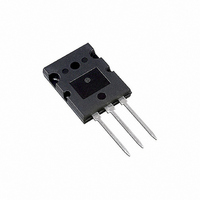
... AMPERES 100 VOLTS mΩ DS(on) N−Channel TO−264 CASE 340G Style 1 MARKING DIAGRAM & PIN ASSIGNMENT MTY100N10E LLYWW 1 3 Gate Source 2 Drain LL = Location Code Y = Year WW = Work Week ORDERING INFORMATION Package Shipping TO−264 25 Units/Rail Publication Order Number: MTY100N10E/D ...

Page 2

ELECTRICAL CHARACTERISTICS Characteristic OFF CHARACTERISTICS Drain−Source Breakdown Voltage ( 250 μ Temperature Coefficient (Positive) Zero Gate Voltage Drain Current (V = 100 Vdc Vdc 100 Vdc, V ...

Page 3

TYPICAL ELECTRICAL CHARACTERISTICS 200 160 120 DRAIN−TO−SOURCE VOLTAGE (VOLTS) DS Figure 1. On−Region Characteristics 0.018 0.016 T ...

Page 4

Switching behavior is most easily modeled and predicted by recognizing that the power MOSFET is charge controlled. The lengths of various switching intervals (Δt) are determined by how fast the FET input capacitance can be charged by current from the ...

Page 5

100 150 Q , TOTAL GATE CHARGE (nC) g Figure 8. Gate Charge versus Gate−to−Source Voltage DRAIN−TO−SOURCE DIODE CHARACTERISTICS 100 0.5 Figure ...

Page 6

SINGLE PULSE T = 25°C C 100 100 μ LIMIT DS(on) THERMAL LIMIT PACKAGE LIMIT 1 0 DRAIN−TO−SOURCE VOLTAGE (VOLTS) DS Figure 11. Maximum Rated Forward Biased ...

Page 7

... Q 3.1 3.5 0.122 0.137 R 2.15 2.35 0.085 0.093 U 6.1 6.5 0.240 0.256 W 2.8 3.2 0.110 0.125 STYLE 1: PIN 1. GATE 2. DRAIN 3. SOURCE ON Semiconductor Website: www.onsemi.com Order Literature: http://www.onsemi.com/orderlit For additional information, please contact your local Sales Representative MTY100N10E/D ...

Related keywords