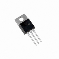
NTP75N03-006 ON Semiconductor, NTP75N03-006 Datasheet

NTP75N03-006
Specifications of NTP75N03-006
Available stocks
Related parts for NTP75N03-006
NTP75N03-006 Summary of contents
Page 1
... CASE 418AA STYLE 5 STYLE 2 3 MARKING DIAGRAMS & PIN ASSIGNMENTS 4 Drain 4 Drain 75N 75N 03−06G 03−06G AYWW AYWW Source 2 Source Gate Drain 2 Drain N75N03−06 = Device Code A = Assembly Location Y = Year WW = Work Week G = Pb−Free Package ORDERING INFORMATION Publication Order Number: NTP75N03−06/D 4 ...
Page 2
... NTP75N03−06 NTP75N03−06G NTB75N03−06 NTB75N03−06G NTB75N03−06T4 NTB75N03−06T4G †For information on tape and reel specifications, including part orientation and tape sizes, please refer to our Tape and Reel Packaging Specifications Brochure, BRD8011/D. NTP75N03−06, NTB75N03−06 Rating = 25°C J (pk Vdc Package TO− ...
Page 3
... Adc Reverse Recovery Time (Note 4) Reverse Recovery Stored Charge (Note 4) 2. Pulse Test: Pulse Width v 300 mS, Duty Cycle v 2%. 3. Switching characteristics are independent of operating junction temperatures. 4. From characterization test data. NTP75N03−06, NTB75N03− 25°C unless otherwise noted) A Symbol V (BR)DSS I DSS ...
Page 4
... I , DRAIN CURRENT (AMPS) D Figure 3. On−Resistance vs. Drain Current and Temperature 1 37 1.4 1.2 1 0.8 0.6 −50 − JUNCTION TEMPERATURE (°C) J Figure 5. On−Resistance Variation Temperature NTP75N03−06, NTB75N03−06 150 ≥ 135 120 105 2 2.6 0 GATE−TO−SOURCE VOLTAGE (VOLTS) GS Figure 2 ...
Page 5
... R , GATE RESISTANCE (W) G Figure 9. Resistive Switching Time Variation vs. Gate Resistance 1600 1400 1200 1000 800 600 400 200 Figure 11. Maximum Avalanche Energy vs. NTP75N03−06, NTB75N03− 25° Figure 8. Gate−to−Source and Drain−to−Source Voltage vs. Total Charge ...
Page 6
... NTP75N03−06, NTB75N03−06 −B− −T− SEATING PLANE 0.13 (0.005) VARIABLE CONFIGURATION ZONE VIEW W−W VIEW W−W 1 10.66 0.42 *For additional information on our Pb−Free strategy and soldering details, please download the ON Semiconductor Soldering and Mounting Techniques Reference Manual, SOLDERRM/D. ...
Page 7
... P.O. Box 61312, Phoenix, Arizona 85082−1312 USA Phone: 480−829−7710 or 800−344−3860 Toll Free USA/Canada Fax: 480−829−7709 or 800−344−3867 Toll Free USA/Canada Email: orderlit@onsemi.com NTP75N03−06, NTB75N03−06 PACKAGE DIMENSIONS TO−220 THREE−LEAD TO−220AB CASE 221A−09 ...


