BSS123LT3 ON Semiconductor, BSS123LT3 Datasheet
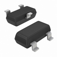
MOSFET N-CH 100V 170MA SOT-23

BSS123LT3

Manufacturer Part Number
BSS123LT3
Description
MOSFET N-CH 100V 170MA SOT-23
Manufacturer
ON Semiconductor
Datasheet

Specifications of BSS123LT3

Fet Type
MOSFET N-Channel, Metal Oxide
Fet Feature
Logic Level Gate
Rds On (max) @ Id, Vgs
6 Ohm @ 100mA, 10V
Drain To Source Voltage (vdss)
100V
Current - Continuous Drain (id) @ 25° C
170mA
Vgs(th) (max) @ Id
2.8V @ 1mA
Input Capacitance (ciss) @ Vds
20pF @ 25V
Power - Max
225mW
Mounting Type
Surface Mount
Package / Case
SOT-23-3, TO-236-3, Micro3™, SSD3, SST3
Lead Free Status / RoHS Status
Contains lead / RoHS non-compliant
Gate Charge (qg) @ Vgs
-

Available stocks

Company
Part Number
Manufacturer
Quantity
Price
Part Number:
BSS123LT3
Manufacturer:
ON SEMICONDUCTOR
Quantity:
30 000
Part Number:
BSS123LT3G
Manufacturer:
ON SEMICONDUCTOR
Quantity:
30 000
BSS123LT1
Power MOSFET
170 mAmps, 100 Volts
N−Channel SOT−23
Features
1. The Power Dissipation of the package may result in a lower continuous drain
2. Pulse Width v 300 ms, Duty Cycle v 2.0%.
3. FR−5 = 1.0  0.75  0.062 in.
March, 2005 − Rev. 5
MAXIMUM RATINGS
Maximum ratings are those values beyond which device damage can occur.
Maximum ratings applied to the device are individual stress limit values (not
normal operating conditions) and are not valid simultaneously. If these limits
are exceeded, device functional operation is not implied, damage may occur
and reliability may be affected.
THERMAL CHARACTERISTICS
Drain−Source Voltage
Gate−Source Voltage
Drain Current
Total Device Dissipation FR−5 Board
Thermal Resistance,
Junction and Storage Temperature
Pb−Free Packages are Available
Semiconductor Components Industries, LLC, 2005
current.
− Continuous
− Non−repetitive (t
− Continuous (Note 1)
− Pulsed (Note 2)
(Note 3) T
Derate above 25 C
Junction−to−Ambient
A
Characteristic
= 25 C
Rating
p
50 ms)
Preferred Device
Symbol
Symbol
T
V
V
R
J
V
I
P
GSM
, T
DSS
DM
I
qJA
GS
D
D
stg
−55 to +150
Value
0.17
0.68
Max
100
225
556
1.8
20
40
1
mW/ C
Unit
Unit
Vdc
Vdc
Vpk
Adc
mW
C/W
C
See detailed ordering and shipping information in the package
dimensions section on page 2 of this data sheet.
Preferred devices are recommended choices for future use
and best overall value.
1
2
ORDERING INFORMATION
SA
M
1
3
http://onsemi.com
PIN ASSIGNMENT
R
170 mAMPS
100 VOLTS
DS(on)
Gate
1
CASE 318
STYLE 21
= Device Code
= Date Code
SOT−23
N−Channel
Drain
Publication Order Number:
3
3
2
= 6 W
Source
2
MARKING
DIAGRAM
BSS123LT1/D
SA

Related parts for BSS123LT3

BSS123LT3 Summary of contents

Page 1

BSS123LT1 Preferred Device Power MOSFET 170 mAmps, 100 Volts N−Channel SOT−23 Features Pb−Free Packages are Available MAXIMUM RATINGS Rating Drain−Source Voltage Gate−Source Voltage − Continuous 50 ms) − Non−repetitive (t p Drain Current − Continuous (Note 1) − Pulsed (Note ...

Page 2

... Pulse Test: Pulse Width v 300 ms, Duty Cycle v 2.0%. ORDERING INFORMATION Device BSS123LT1 BSS123LT1G BSS123LT3 BSS123LT3G †For information on tape and reel specifications, including part orientation and tape sizes, please refer to our Tape and Reel Packaging Specifications Brochure, BRD8011/D. BSS123LT1 ( unless otherwise noted) ...

Page 3

TYPICAL ELECTRICAL CHARACTERISTICS 2.0 1 1.6 1.4 1.2 1.0 0.8 0.6 0.4 0 1.0 2.0 3.0 4.0 5.0 6 DRAN SOURCE VOLTAGE (VOLTS) DS Figure 1. Ohmic Region 2.4 2.2 V ...

Page 4

... *For additional information on our Pb−Free strategy and soldering details, please download the ON Semiconductor Soldering and Mounting Techniques Reference Manual, SOLDERRM/D. ON Semiconductor and are registered trademarks of Semiconductor Components Industries, LLC (SCILLC). SCILLC reserves the right to make changes without further notice to any products herein. SCILLC makes no warranty, representation or guarantee regarding the suitability of its products for any particular purpose, nor does SCILLC assume any liability arising out of the application or use of any product or circuit, and specifically disclaims any and all liability, including without limitation special, consequential or incidental damages. “ ...

Related keywords