NTMFS4120NT1G ON Semiconductor, NTMFS4120NT1G Datasheet
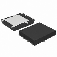
MOSFET N-CHAN 18A 30V SO8 FL

NTMFS4120NT1G

Manufacturer Part Number
NTMFS4120NT1G
Description
MOSFET N-CHAN 18A 30V SO8 FL
Manufacturer
ON Semiconductor
Datasheet

Specifications of NTMFS4120NT1G

Fet Type
MOSFET N-Channel, Metal Oxide
Fet Feature
Logic Level Gate
Rds On (max) @ Id, Vgs
4.5 mOhm @ 26A, 10V
Drain To Source Voltage (vdss)
30V
Current - Continuous Drain (id) @ 25° C
11A
Vgs(th) (max) @ Id
2.5V @ 250µA
Gate Charge (qg) @ Vgs
50nC @ 4.5V
Input Capacitance (ciss) @ Vds
3600pF @ 24V
Power - Max
900mW
Mounting Type
Surface Mount
Package / Case
5-DFN, SO8 FL
Lead Free Status / RoHS Status
Lead free / RoHS Compliant
Other names
NTMFS4120NT1G
NTMFS4120NT1GOSTR

Available stocks

Company
Part Number
Manufacturer
Quantity
Price
Part Number:
NTMFS4120NT1G
Manufacturer:
ON/安森美
Quantity:
20 000
NTMFS4120N
Power MOSFET
30 V, 31 A, Single N-Channel,
SO-8 Flat Lead
Features
Applications
Stresses exceeding Maximum Ratings may damage the device. Maximum
Ratings are stress ratings only. Functional operation above the Recommended
Operating Conditions is not implied. Extended exposure to stresses above the
Recommended Operating Conditions may affect device reliability.
1. Surface mounted on FR4 board using 1 in sq pad size
2. Surface mounted on FR4 board using the minimum recommended pad size
© Semiconductor Components Industries, LLC, 2007
July, 2007 - Rev. 3
MAXIMUM RATINGS
Power Dissipation (Note 2)
THERMAL RESISTANCE MAXIMUM RATINGS
Drain-to-Source Voltage
Gate-to-Source Voltage
Continuous Drain Current
Power Dissipation (Note 1)
Continuous Drain Current
Pulsed Drain Current
Operating Junction and Storage Temperature
Source Current (Body Diode)
Single Pulse Drain-to-Source Avalanche Energy
Lead Temperature for Soldering Purposes
Junction-to-Case - Steady State
Junction-to-Ambient - Steady State (Note 1)
Junction-to-Ambient - t v10 s (Note 1)
Junction-to-Ambient - Steady State (Note 2)
Low R
Optimized Gate Charge
Low Inductance SO-8 Package
These are Pb-Free Devices
Notebooks, Graphics Cards
DC-DC Converters
Synchronous Rectification
(Cu area = 1.127 in sq [1 oz] including traces).
(Cu area = 1.0 in sq).
(Note 1 )
(Note 2)
(V
L = 1 mH, R
(1/8″ from case for 10 s)
DD
= 30 V, V
DS(on)
G
= 25 W)
GS
Parameter
Parameter
= 10 V, I
(T
J
= 25°C unless otherwise noted)
t v10 s
t v10 s
PK
Steady
Steady
Steady
State
State
State
= 30 A,
t
p
= 10 ms
T
T
T
T
T
T
T
A
A
A
A
A
A
A
= 25°C
= 85°C
= 25°C
= 25°C
= 25°C
= 85°C
= 25°C
Symbol
Symbol
T
V
R
R
R
R
J
V
E
I
P
P
, T
T
DSS
DM
I
I
I
qJC
qJA
qJA
qJA
GS
AS
D
D
S
D
D
L
stg
-55 to
Value
Value
139.1
$20
55.8
150
450
260
2.2
6.9
8.0
0.9
7.0
1.7
30
18
13
31
94
18
11
1
°C/W
Unit
Unit
mJ
°C
°C
W
W
V
V
A
A
A
A
†For information on tape and reel specifications,
NTMFS4120NT1G
NTMFS4120NT3G
SO-8 FLAT LEAD
including part orientation and tape sizes, please
refer to our Tape and Reel Packaging Specification
Brochure, BRD8011/D.
V
CASE 488AA
(BR)DSS
30 V
(Note: Microdot may be in either location)
STYLE 1
Device
4120N = Specific Device Code
A
Y
WW
G
ORDERING INFORMATION
G
1
http://onsemi.com
4.2 mW @ 4.5 V
3.5 mW @ 10 V
= Assembly Location
= Year
= Work Week
= Pb-Free Package
R
(Pb-Free)
(Pb-Free)
DS(on)
Package
SO-8 FL
SO-8 FL
D
Publication Order Number:
Typ
S
S
S
S
G
1500 Tape & Reel
5000 Tape & Reel
MARKING
DIAGRAM
NTMFS4120N/D
AYWWG
Shipping
4120N
D
D
G
(Note 1)
I
D
31 A
Max
D
D

Related parts for NTMFS4120NT1G

NTMFS4120NT1G Summary of contents

Page 1

... P 0 ° - stg 150 I 7 450 mJ AS °C T 260 L Symbol Value Unit °C/W R 1.7 NTMFS4120NT1G qJC 55.8 R qJA R 18 NTMFS4120NT3G qJA R 139.1 qJA †For information on tape and reel specifications, 1 http://onsemi.com Typ (BR)DSS DS(on) (Note MARKING DIAGRAM D S ...

Page 2

ELECTRICAL CHARACTERISTICS Characteristic OFF CHARACTERISTICS Drain-to-Source Breakdown Voltage Drain-to-Source Breakdown Voltage emperature Coefficient T Zero Gate Voltage Drain Current Gate-to-Source Leakage Current ON CHARACTERISTICS (Note 3) Gate Threshold Voltage Negative Threshold Temperature Coefficient Drain-to-Source On Resistance Forward Transconductance CHARGES, CAPACITANCES ...

Page 3

DRAIN-TO-SOURCE VOLTAGE (VOLTS) DS Figure 1. On-Region Characteristics 0.008 0.007 T = ...

Page 4

C iss 4000 3000 2000 C oss 1000 C rss GATE-TO-SOURCE OR DRAIN-TO-SOURCE VOLTAGE (VOLTS) Figure 7. Capacitance Variation 1000 4.5 ...

Page 5

D = 0.5 0.2 0.1 0.1 0.05 0.02 0.01 0.01 SINGLE PULSE 0.001 1E-04 1E-03 1E-02 NTMFS4120N 1E-01 1E+00 t, TIME (seconds) Figure 13. Thermal Response http://onsemi.com 5 1E+01 1E+02 1E+03 ...

Page 6

... M 3.200 *For additional information on our Pb-Free strategy and soldering details, please download the ON Semiconductor Soldering and Mounting Techniques Reference Manual, SOLDERRM/D. N. American Technical Support: 800-282-9855 Toll Free  USA/Canada Europe, Middle East and Africa Technical Support:  Phone: 421 33 790 2910 Japan Customer Focus Center   ...

Related keywords