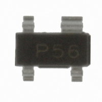
HSMS-2855-BLKG Avago Technologies US Inc., HSMS-2855-BLKG Datasheet - Page 5

HSMS-2855-BLKG
Manufacturer Part Number
HSMS-2855-BLKG
Description
DIODE SCHOTTKY DETECT SS SOT-143
Manufacturer
Avago Technologies US Inc.
Specifications of HSMS-2855-BLKG
Package / Case
SOT-143, SOT-143B, TO-253AA
Diode Type
Schottky - 2 Independent
Voltage - Peak Reverse (max)
2V
Capacitance @ Vr, F
0.3pF @ 1V, 1MHz
Configuration
Unconnected Pair
Frequency Range
UHF
Maximum Diode Capacitance
0.3 pF (Typ)
Maximum Operating Temperature
+ 150 C
Minimum Operating Temperature
- 65 C
Maximum Forward Voltage
0.25 V @ 1 mA
Mounting Style
SMD/SMT
Typical Voltage Sensitivity
40 mV/uW @915MHz
Capacitance, Junction
0.3 pF
Current, Reverse
175 μA
Package Type
SOT-23 (SOT-143)
Primary Type
Schottky Barrier
Resistance, Thermal, Junction To Case
500 °C/W
Speed, Switching
RF
Temperature, Junction, Maximum
+150 °C
Temperature, Operating
-65 to +150 °C
Voltage, Forward
250 mV
Voltage, Reverse
3.8 V
Diode Case Style
SOT-143
No. Of Pins
3
Forward Current If
1mA
Forward Voltage
250mV
Leaded Process Compatible
Yes
Rohs Compliant
Yes
Forward Current If Max
1mA
Forward Voltage Vf Max
250mV
Capacitance Ct
0.3pF
Lead Free Status / RoHS Status
Lead free / RoHS Compliant
Current - Max
-
Power Dissipation (max)
-
Resistance @ If, F
-
Lead Free Status / Rohs Status
Lead free / RoHS Compliant
Other names
516-1933
HSMS-2855-BLKG
HSMS-2855-BLKG
Available stocks
Company
Part Number
Manufacturer
Quantity
Price
Part Number:
HSMS-2855-BLKG
Manufacturer:
AVAGO/安华高
Quantity:
20 000
Applications Information
Introduction
Avago’s HSMS-285x family of Schottky detector diodes
has been developed specifically for low cost, high
volume designs in small signal (P
tions at frequencies below 1.5 GHz. At higher frequen-
cies, the DC biased HSMS-286x family should be consid-
ered.
In large signal power or gain control applications
(P
ucts should be used. The HSMS-285x zero bias diode is
not designed for large signal designs.
Schottky Barrier Diode Characteristics
Stripped of its package, a Schottky barrier diode chip
consists of a metal-semiconductor barrier formed by de-
position of a metal layer on a semiconductor. The most
common of several different types, the passivated diode,
is shown in Figure 5, along with its equivalent circuit.
Figure 5. Schottky Diode Chip.
R
of the bondwire and leadframe resistance, the resistance
of the bulk layer of silicon, etc. RF energy coupled into
R
output of the diode. C
of the diode, controlled by the thickness of the epitaxial
layer and the diameter of the Schottky contact. R
junction resistance of the diode, a function of the total
current flowing through it.
where
I
from picoamps for high barrier diodes to as much as 5
µA for very low barrier diodes.
5
N-TYPE OR P-TYPE SILICON SUBSTRATE
S
S
S
in
PASSIVATION
N-TYPE OR P-TYPE EPI
n = ideality factor (see table of SPICE parameters)
T = temperature in °K
I
I
is a function of diode barrier height, and can range
is the parasitic series resistance of the diode, the sum
is lost as heat — it does not contribute to the rectified
S
b
> -20 dBm), the HSMS-282x and HSMS-286x prod-
= saturation current (see table of SPICE parameters)
= externally applied bias current in amps
CROSS-SECTION OF SCHOTTKY
I = I
R
BARRIER DIODE CHIP
j
=
=
S
R
(exp
S
= R
8.33 X 10
R ≈
METAL
SCHOTTKY JUNCTION
V
0.026
I
d
S
I
(
26,000
S
+ I
HSMS-285A/6A fig 9
–
0.026
V - IR
I
+ I
S
LAYER
b
+ I
0.026
PASSIVATION
at 25°C
b
-5
I
b
S
f
J
n T
is parasitic junction capacitance
)
- 1)
= R
V
– R
EQUIVALENT
C
s
j
in
R
CIRCUIT
S
< -20 dBm) applica-
R
j
j
is the
The Height of the Schottky Barrier
The current-voltage characteristic of a Schottky barrier
diode at room temperature is described by the following
equation:
On a semi-log plot (as shown in the Avago catalog) the
current graph will be a straight line with inverse slope
2.3 X 0.026 = 0.060 volts per cycle (until the effect of R
seen in a curve that droops at high current). All Schottky
diode curves have the same slope, but not necessar-
ily the same value of current for a given voltage. This is
determined by the saturation current, I
the barrier height of the diode.
Through the choice of p-type or n-type silicon, and the
selection of metal, one can tailor the characteristics of a
Schottky diode. Barrier height will be altered, and at the
same time C
low barrier height diodes (with high values of I
able for zero bias applications) are realized on p-type
silicon. Such diodes suffer from higher values of R
do the n-type. Thus, p-type diodes are generally reserved
for small signal detector applications (where very high
values of R
used for mixer applications (where high L.O. drive levels
keep R
Measuring Diode Parameters
The measurement of the five elements which make up
the low frequency equivalent circuit for a packaged
Schottky diode (see Figure 6) is a complex task. Various
techniques are used for each element. The task begins
with the elements of the diode chip itself.
FOR THE HSMS-285x SERIES
C
L
C
R
R
Figure 6. Equivalent Circuit of a Schottky Diode.
I = I
P
R
P
j
S
V
= 2 nH
= 0.18 pF
= 0.08 pF
= 25 Ω
= 9 KΩ
j
=
=
S
R
L
(exp
S
P
= R
V
8.33 X 10
R ≈
low).
V
0.026
I
S
d
(
I
S
26,000
+ I
–
V
0.026
V - IR
I
R
+ I
S
swamp out high R
J
b
S
0.026
+ I
and R
b
at 25°C
-5
I
b
f
S
n T
)
C
- 1)
S
= R
P
will be changed. In general, very
V
R
– R
V
C
j
s
S
) and n-type diodes are
S
, and is related to
S
S
, suit-
than
S
is


