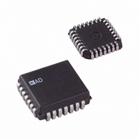
DAC8412FPC Analog Devices Inc, DAC8412FPC Datasheet - Page 7

DAC8412FPC
Manufacturer Part Number
DAC8412FPC
Description
DAC 4-CH R-2R 12-Bit 28-Pin PLCC
Manufacturer
Analog Devices Inc
Datasheet
1.DAC8412FPCZ.pdf
(20 pages)
Specifications of DAC8412FPC
Package
28PLCC
Resolution
12 Bit
Conversion Rate
167 KSPS
Architecture
R-2R
Digital Interface Type
Parallel
Number Of Outputs Per Chip
4
Output Type
Voltage
Full Scale Error
±8 LSB
Integral Nonlinearity Error
±4 LSB
Maximum Settling Time
10(Typ) us
Rohs Status
RoHS non-compliant
Settling Time
6µs
Number Of Bits
12
Data Interface
Parallel
Number Of Converters
4
Voltage Supply Source
Single Supply
Power Dissipation (max)
330mW
Operating Temperature
-40°C ~ 85°C
Mounting Type
Surface Mount
Package / Case
28-LCC (J-Lead)
Number Of Channels
4
Interface Type
Parallel
Single Supply Voltage (typ)
5V
Dual Supply Voltage (typ)
±15V
Power Supply Requirement
Single/Dual
Single Supply Voltage (min)
4.75V
Single Supply Voltage (max)
5.25V
Dual Supply Voltage (min)
±14.25V
Dual Supply Voltage (max)
±15.75V
Operating Temp Range
-40C to 85C
Operating Temperature Classification
Industrial
Mounting
Surface Mount
Pin Count
28
Package Type
PLCC
Lead Free Status / Rohs Status
Not Compliant
Available stocks
Company
Part Number
Manufacturer
Quantity
Price
Company:
Part Number:
DAC8412FPC
Manufacturer:
AD
Quantity:
1 000
Company:
Part Number:
DAC8412FPC
Manufacturer:
Analog Devices Inc
Quantity:
10 000
Part Number:
DAC8412FPC
Manufacturer:
ADI/亚德诺
Quantity:
20 000
Company:
Part Number:
DAC8412FPC-REEL
Manufacturer:
Analog Devices Inc
Quantity:
10 000
Company:
Part Number:
DAC8412FPCZ
Manufacturer:
TI
Quantity:
650
Company:
Part Number:
DAC8412FPCZ
Manufacturer:
ADI33
Quantity:
176
Company:
Part Number:
DAC8412FPCZ
Manufacturer:
Analog Devices Inc
Quantity:
10 000
Part Number:
DAC8412FPCZ
Manufacturer:
ADI/亚德诺
Quantity:
20 000
Company:
Part Number:
DAC8412FPCZ-REEL
Manufacturer:
Analog Devices Inc
Quantity:
10 000
ABSOLUTE MAXIMUM RATINGS
T
Table 3.
Parameter
V
V
V
V
V
V
Current into Any V
Digital Input Voltage to DGND
Digital Output Voltage to DGND
Operating Temperature Range
Junction Temperature
Storage Temperature Range
Power Dissipation Package
Lead Temperature
Stresses above those listed under Absolute Maximum Ratings
may cause permanent damage to the device. This is a stress
rating only; functional operation of the device at these or any
other conditions above those indicated in the operational
section of this specification is not implied. Exposure to absolute
maximum rating conditions for extended periods may affect
device reliability.
SS
SS
LOGIC
SS
REFH
REFH
A
EP, FP, FPC
AT, BT, BTC
Soldering
= +25°C, unless otherwise noted.
to V
to V
to V
to V
to V
to DGND
DD
LOGIC
REFL
DD
REFL
SS
pin
Rating
−0.3 V, +33.0 V
−0.3 V, +33.0 V
−0.3 V, +7.0 V
−0.3 V, +V
+2.0 V, +33.0 V
+2.0 V, V
±15 mA
−0.3 V, V
−0.3 V, +7.0 V
−40°C to +85°C
−55°C to +125°C
150°C
−65°C to +150°C
1000 mW
JEDEC Industry Standard
J-STD-020
SS
LOGIC
SS
− V
− 2.0 V
+ 0.3 V
DD
Rev. F | Page 7 of 20
THERMAL RESISTANCE
θ
device in socket.
Table 4. Thermal Resistance
Package Type
28-Lead Plastic DIP (PDIP)
28-Terminal Ceramic Leadless Chip Carrier (LLC)
28-Lead Plastic Leaded Chip Carrier (PLLC)
28-Lead Ceramic Dual In-Line Package (CERDIP)
ESD CAUTION
JA
is specified for the worst-case mounting conditions, that is, a
DAC8412/DAC8413
θ
48
70
63
51
JA
θ
22
28
25
9
JC
Unit
°C/W
°C/W
°C/W
°C/W


