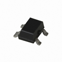
ATF-54143-BLKG Avago Technologies US Inc., ATF-54143-BLKG Datasheet - Page 13

ATF-54143-BLKG
Manufacturer Part Number
ATF-54143-BLKG
Description
IC PHEMT 2GHZ 3V 60MA SOT-343
Manufacturer
Avago Technologies US Inc.
Datasheet
1.ATF-54143-TR2G.pdf
(17 pages)
Specifications of ATF-54143-BLKG
Package / Case
SC-70-4, SC-82-4, SOT-323-4, SOT-343
Transistor Type
pHEMT FET
Frequency
2GHz
Gain
16.6dB
Voltage - Rated
5V
Current Rating
120mA
Noise Figure
0.5dB
Current - Test
60mA
Voltage - Test
3V
Power - Output
20.4dBm
Configuration
Single Dual Source
Transistor Polarity
N-Channel
Power Dissipation
725 mW
Drain Source Voltage Vds
5 V
Gate-source Breakdown Voltage
- 5 V to 1 V
Continuous Drain Current
120 mA
Maximum Operating Temperature
+ 150 C
Maximum Drain Gate Voltage
- 5 V to 1 V
Minimum Operating Temperature
- 65 C
Mounting Style
SMD/SMT
Continuous Drain Current Id
120mA
Power Dissipation Pd
725mW
Noise Figure Typ
0.5dB
Rf Transistor Case
SOT-343
No. Of Pins
4
Frequency Max
6GHz
Rohs Compliant
Yes
Drain Current Idss Max
60mA
Lead Free Status / RoHS Status
Lead free / RoHS Compliant
Lead Free Status / RoHS Status
Lead free / RoHS Compliant, Lead free / RoHS Compliant
Other names
516-1868
ATF-54143-BLKG
ATF-54143-BLKG
Available stocks
Company
Part Number
Manufacturer
Quantity
Price
Company:
Part Number:
ATF-54143-BLKG
Manufacturer:
AVAGO
Quantity:
30 000
Part Number:
ATF-54143-BLKG
Manufacturer:
AVAGO/安华高
Quantity:
20 000
Designing with S and Noise
Parameters and the Non-Linear Model
The non-linear model describing
the ATF-54143 includes both the
die and associated package
model. The package model
includes the effect of the pins but
does not include the effect of the
additional source inductance
associated with grounding the
source leads through the printed
circuit board. The device S and
Noise Parameters do include the
effect of 0.020 inch thickness
printed circuit board vias. When
comparing simulation results
between the measured S param-
Figure 3. Adding Vias to the ATF-54143 Non-Linear Model for Comparison to Measured S and Noise Parameters.
13
VIA2
V1
D=20.0 mil
H=25.0 mil
T=0.15 mil
Rho=1.0
W=40.0 mil
VIA2
V2
D=20.0 mil
H=25.0 mil
T=0.15 mil
Rho=1.0
W=40.0 mil
SOURCE
DRAIN
A T F - 5 4 1 4 3
eters and the simulated non-
linear model, be sure to include
the effect of the printed circuit
board to get an accurate compari-
son. This is shown schematically
in Figure 3.
For Further Information
The information presented here is
an introduction to the use of the
ATF-54143 enhancement mode
PHEMT. More detailed application
circuit information is available
from Agilent Technologies.
Consult the web page or your
local Agilent Technologies sales
representative.
SOURCE
GATE
VIA2
V4
D=20.0 mil
H=25.0 mil
T=0.15 mil
Rho=1.0
W=40.0 mil
VIA2
V3
D=20.0 mil
H=25.0 mil
T=0.15 mil
Rho=1.0
W=40.0 mil
MSUB
MSub1
H=25.0 mil
Er=9.6
Mur=1
Cond=1.0E+50
Hu=3.9e+034 mil
T=0.15 mil
TanD=0
Rough=0 mil
MSub


