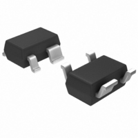
ATF-35143-TR2G Avago Technologies US Inc., ATF-35143-TR2G Datasheet - Page 2

ATF-35143-TR2G
Manufacturer Part Number
ATF-35143-TR2G
Description
IC PHEMT 1.9GHZ 15MA LN SOT-343
Manufacturer
Avago Technologies US Inc.
Datasheet
1.ATF-35143-TR2G.pdf
(19 pages)
Specifications of ATF-35143-TR2G
Transistor Type
pHEMT FET
Frequency
2GHz
Gain
18dB
Voltage - Rated
5.5V
Current Rating
80mA
Noise Figure
0.4dB
Current - Test
15mA
Voltage - Test
2V
Power - Output
10dBm
Package / Case
SC-70-4, SC-82-4, SOT-323-4, SOT-343
Channel Type
N
Configuration
Single Dual Source
Gate-source Voltage (max)
5V
Drain Current (max)
80mA
Operating Temperature Classification
Military
Mounting
Surface Mount
Pin Count
4 +Tab
Package Type
SOT-343
Lead Free Status / RoHS Status
Lead free / RoHS Compliant
Available stocks
Company
Part Number
Manufacturer
Quantity
Price
Part Number:
ATF-35143-TR2G
Manufacturer:
AVAGO/安华高
Quantity:
20 000
ATF-35143 Absolute Maximum Ratings
Notes:
6. Under large signal conditions, VGS may swing positive and the drain current may exceed Idss. These conditions are acceptable as long as the
7. Distribution data sample size is 450 samples taken from 9 different wafers. Future wafers allocated to this product may have nominal values
8. Measurements made on production test board. This circuit represents a trade-off between an optimal noise match and a realizeable match
Product Consistency Distribution Charts
2
Figure 1. Typical Pulsed I-V Curves
(V
200
160
120
120
100
Figure 3. NF @ 2 GHz, 2 V, 15 mA.
LSL=0.2, Nominal=0.37, USL=0.7
80
40
80
60
40
20
GS
maximum Pdiss and Pin max ratings are not exceeded.
anywhere within the upper and lower spec limits.
based on production test requirements. Circuit losses have been de-embedded from actual measurements.
0
0
0.2
Symbol
= -0.2 V per step)
P
0
P
T
in max
V
V
T
V
I
θ
STG
DS
diss
GD
DS
GS
CH
-3 Std
jc
0.3
2
0.4
NF (dB)
Drain - Source Voltage
Gate - Source Voltage
Gate Drain Voltage
Drain Current
Total Power Dissipation
RF Input Power
Channel Temperature
Storage Temperature
Thermal Resistance
V
Parameter
DS
+3 Std
4
(V)
0.5
[6]
.
0.6
6
+0.6 V
–0.6 V
[2]
0 V
0.7
[2]
8
[5]
Cpk = 3.7
Std = 0.03
[2]
[2]
[4]
[1]
[7, 8]
°C/W
Units
dBm
mW
mA
°C
°C
V
V
V
120
100
160
120
Figure 2. OIP3 @ 2 GHz, 2 V, 15 mA.
LSL=19.0, Nominal=20.9, USL=23.0
80
60
40
20
Figure 4. Gain @ 2 GHz, 2 V, 15 mA.
LSL=16.5, Nominal=18.0, USL=19.5
80
40
0
0
19
16
-3 Std
-65 to 160
20
Maximum
Absolute
17
I
dss
300
160
150
5.5
14
-5
-5
-3 Std
[3]
OIP3 (dBm)
GAIN (dB)
21
18
+3 Std
22
+3 Std
19
Notes:
1. Operation of this device above any
2. Assumes DC quiesent conditions.
3. V
4. Source lead temperature is 25°C.
5. Thermal resistance measured using
23
one of these parameters may cause
permanent damage.
Derate 3.2 mW/°C for T
QFI Measurement method.
GS
24
20
= 0 V
Cpk = 1.73
Std = 0.35
Cpk = 2.75
Std = 0.17
L
> 67°C.


