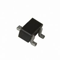
NE68019-T1-A CEL, NE68019-T1-A Datasheet - Page 2

NE68019-T1-A
Manufacturer Part Number
NE68019-T1-A
Description
TRANSISTOR NPN 2GHZ SMD
Manufacturer
CEL
Datasheet
1.NE68019-T1-A.pdf
(20 pages)
Specifications of NE68019-T1-A
Transistor Type
NPN
Voltage - Collector Emitter Breakdown (max)
10V
Frequency - Transition
10GHz
Noise Figure (db Typ @ F)
1.7dB ~ 1.9dB @ 1GHz ~ 2GHz
Gain
9.6dB ~ 13.5dB
Power - Max
100mW
Dc Current Gain (hfe) (min) @ Ic, Vce
80 @ 5mA, 3V
Current - Collector (ic) (max)
35mA
Mounting Type
Surface Mount
Package / Case
Surface Mount
Configuration
Single
Transistor Polarity
NPN
Continuous Collector Current
0.035 A
Power Dissipation
0.1 W
Lead Free Status / RoHS Status
Lead free / RoHS Compliant
Other names
2SC5008-T1-A
NE68019-ATR
NE68019-ATR
Available stocks
Company
Part Number
Manufacturer
Quantity
Price
Company:
Part Number:
NE68019-T1-A
Manufacturer:
RENESAS
Quantity:
5 700
Company:
Part Number:
NE68019-T1-A
Manufacturer:
CEL
Quantity:
3 000
ELECTRICAL CHARACTERISTICS
ELECTRICAL CHARACTERISTICS
Notes:
1. Electronic Industrial Association of Japan.
2. Pulsed measurement, PW≤350 μs, duty cycle ≤2%.
3. The emitter terminal should be connected to the ground
SYMBOLS
SYMBOLS
R
R
R
R
|S
|S
TH (J- C)
MAG
GNF
C
TH (J-A)
MAG
TH (J- C)
I
I
GNF
TH (J-A)
I
I
Cre
h
NF
CBO
EBO
h
P
CBO
21E
NF
EBO
P
f
RE
21E
FE
f
T
FE
T
T
T
3
3
|
|
2
2
Gain Bandwidth Product at V
Noise Figure at V
Associated Gain at V
Maximum Available Gain at V
Insertion Power Gain at V
Forward Current Gain
Collector Cutoff Current at V
Emitter Cutoff Current at V
Feedback Capacitance at V
Total Power Dissipation
Thermal Resistance (Junction to Ambient)
Thermal Resistance (Junction to Case)
Gain Bandwidth Product at V
Noise Figure at V
Associated Gain at V
Maximum Available Gain at V
Insertion Power Gain at V
Forward Current Gain
Collector Cutoff Current at V
Emitter Cutoff Current at V
Feedback Capacitance at
V
V
Total Power Dissipation
Thermal Resistance (Junction to Ambient)
Thermal Resistance (Junction to Case)
CB
CE
= 3V, I
= 10 V, I
EIAJ
PARAMETERS AND CONDITIONS
PACKAGE OUTLINE
1
E
PARAMETERS AND CONDITIONS
REGISTERED NUMBER
= 0 mA, f = 1 MHz
E
PART NUMBER
EIAJ
= 0 mA, f = 1 MHz
CE
CE
PACKAGE OUTLINE
1
REGISTERED NUMBER
= 6 V, I
= 6 V, I
CE
CE
PART NUMBER
2
2
at V
at V
= 6 V, I
= 6 V, I
CE
CE
V
EB
V
EB
CE
C
CE
C
CB
CE
CB
CE
= 6 V, I
CB
CE
= 6 V, I
= 5 mA, f = 1 GHz
CE
CE
= 1V, I
= 5 mA, f = 1 GHz
CE
= 1V, I
= 6 V, I
= 6 V, I
= 1 V, I
C
= 3 V, I
= 10 V, I
= 3 V, I
C
= 10 V, I
= 6 V, I
= 6 V, I
= 6 V, I
= 6 V, I
= 5 mA,
= 5 mA,
C
C
C
C
C
= 10 mA,
= 0 mA
C
E
= 0 mA
= 10 mA,
C
C
f = 2 GHz
f = 4 GHz
f = 1 GHz
f = 2 GHz
f = 4 GHz
f = 1 GHz
f = 2 GHz
f = 4 GHz
f = 1 GHz
f = 2 GHz
f = 4 GHz
f = 2 GHz
f = 4 GHz
f = 1 GHz
f = 2 GHz
f = 4 GHz
f = 1 GHz
f = 2 GHz
f = 4 GHz
f = 1 GHz
f = 2 GHz
f = 2 GHz
C
= 10 mA
C
= 10 mA
(T
C
= 0 mA, f = 1 MHz
E
= 5 mA
(T
C
E
= 5 mA
= 10 mA
= 10 mA
= 10 mA
= 0 mA
A
= 10 mA
= 0 mA
A
= 25°C)
= 25°C)
UNITS MIN TYP MAX MIN TYP MAX MIN TYP MAX MIN TYP MAX
°C/W
°C/W
GHz
mW
dB
dB
dB
dB
dB
dB
dB
dB
dB
dB
dB
dB
μA
μA
pF
pF
50 100 250
UNITS MIN
°C/W
NE68030
GHz
°C/W
mW
2SC4228
dB
dB
dB
dB
dB
dB
dB
dB
dB
dB
dB
dB
μA
μA
pF
12.5
10.9
13.5
1.5
1.7
2.9
9.4
5.3
6.8
8.5
3.6
0.3
10
17
terminal of the 3 terminal capacitance bridge.
30
10.5 12.5
50
150
833
200
1.0
1.0
0.7
00 (CHIP)
NE68000
12.5
18.5
16.2
10.2
TYP MAX MIN
100
1.7
2.6
7.5
10
17
50
8
NE68033
2SC3585
10.9
11.0
100 250
1.6
1.8
2.1
9.0
4.2
6.7
6.7
3.7
0.3
250
400
120
10
17
13
2.4
1.0
1.0
33
200
620
200
3.0
1.0
1.0
0.8
7.5
50
NE68018
10.5 12.5
2SC5013
50
10.2
12.7
15.5
TYP MAX MIN
100
1.6
1.8
8.2
9.8
4.6
0.3
10
14
19
18
NE68035
2SC3587
12.5
18.5
16.2
10.2
100 250
1.7
2.6
7.5
0.2
10
17
35
8
250
150
833
200
1.0
1.0
0.7
3
290
550
200
2.4
1.0
1.0
0.7
80
50
NE68039/39R
NE68019
2SC5008
13.5
18.5
11.8
TYP MAX
2SC4095
1.7
1.9
9.6
7.3
9.2
4.4
0.3
10
15
19
12.4
14.5
0.25 0.8
100 250
1.7
2.6
6.5
8.7
9.6
4.9
10
18
11
39
1000
160
100
200
1.0
1.0
0.7
200
620
200
2.5
1.0
1.0


