ST380CH06C0 Vishay, ST380CH06C0 Datasheet - Page 2
ST380CH06C0
Manufacturer Part Number
ST380CH06C0
Description
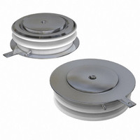
SCR PHASE CONT 600V 960A E-PUK
Manufacturer
Vishay
Specifications of ST380CH06C0
Scr Type
Standard Recovery
Voltage - Off State
600V
Voltage - Gate Trigger (vgt) (max)
3V
Voltage - On State (vtm) (max)
1.58V
Current - On State (it (av)) (max)
960A
Current - On State (it (rms)) (max)
2220A
Current - Gate Trigger (igt) (max)
200mA
Current - Hold (ih) (max)
600mA
Current - Off State (max)
100mA
Current - Non Rep. Surge 50, 60hz (itsm)
12500A, 13000A
Operating Temperature
-40°C ~ 150°C
Mounting Type
Chassis Mount
Package / Case
TO-200AB, E-PUK
Current - On State (it (rms) (max)
2220A
Mounting Style
SMD/SMT
Peak Repetitive Off-state Voltage, Vdrm
600V
Gate Trigger Current Max, Igt
200mA
Current It Av
960A
On State Rms Current It(rms)
2.22kA
Peak Non Rep Surge Current Itsm 50hz
12.5kA
Lead Free Status / RoHS Status
Lead free / RoHS Compliant
Other names
*ST380CH06C0
VS-ST380CH06C0
VS-ST380CH06C0
VSST380CH06C0
VSST380CH06C0
VS-ST380CH06C0
VS-ST380CH06C0
VSST380CH06C0
VSST380CH06C0
Available stocks
Company
Part Number
Manufacturer
Quantity
Price
Company:

Part Number:
ST380CH06C0
Manufacturer:
RENESAS
Quantity:
660
Company:
Part Number:
ST380CH06C0
Manufacturer:
Vishay Semiconductors
Quantity:
135


ST380CHPbF Series
Vishay High Power Products
www.vishay.com
2
ABSOLUTE MAXIMUM RATINGS
PARAMETER
Maximum average on-state current
at heatsink temperature
Maximum RMS on-state current
Maximum peak, one-cycle
non-repetitive surge current
Maximum I
Maximum I
Low level value of threshold voltage
High level value of threshold voltage
Low level value of on-state slope resistance
High level value of on-state slope resistance
Maximum on-state voltage
Maximum holding current
Typical latching current
SWITCHING
PARAMETER
Maximum non-repetitive rate of rise
of turned-on current
Typical delay time
Typical turn-off time
BLOCKING
PARAMETER
Maximum critical rate of rise of
off-state voltage
Maximum peak reverse and
off-state leakage current
2
2
t for fusing
√t for fusing
For technical questions, contact: ind-modules@vishay.com
SYMBOL
SYMBOL
SYMBOL
(Hockey PUK Version), 960 A
V
V
I
T(RMS)
dV/dt
I
I
dI/dt
I
I
T(TO)1
T(TO)2
V
RRM
T(AV)
I
DRM
TSM
I
2
r
r
t
t
I
I
2
TM
t1
t2
H
d
q
Phase Control Thyristors
√t
L
t
,
Gate drive 20 V, 20 Ω, t
T
Gate current 1 A, dI
V
I
V
T
T
180° conduction, half sine wave
double side (single side) cooled
DC at 25 °C heatsink temperature double side cooled
t = 10 ms
t = 8.3 ms
t = 10 ms
t = 8.3 ms
t = 10 ms
t = 8.3 ms
t = 10 ms
t = 8.3 ms
t = 0.1 to 10 ms, no voltage reapplied
(16.7 % x π x I
(I > π x I
(16.7 % x π x I
(I > π x I
I
T
TM
pk
J
J
d
R
J
J
= T
= 0.67 % V
= T
= T
= 25 °C, anode supply 12 V resistive load
= 2900 A, T
= 50 V, dV/dt = 20 V/µs, gate 0 V 100 Ω, t
= 550 A, T
J
J
J
maximum linear to 80 % rated V
maximum, anode voltage ≤ 80 % V
maximum, rated V
T(AV)
T(AV)
), T
), T
DRM
J
No voltage
reapplied
100 % V
reapplied
No voltage
reapplied
100 % V
reapplied
T(AV)
T(AV)
J
= T
J
J
= T
TEST CONDITIONS
TEST CONDITIONS
TEST CONDITIONS
= T
= T
, T
J
< I < π x I
< I < π x I
g
J
J
maximum, dI/dt = 40 A/µs,
/dt = 1 A/µs
J
J
maximum, t
= 25 °C
maximum
maximum
RRM
RRM
r
≤ 1 µs
DRM
T(AV)
T(AV)
Sinusoidal half wave,
initial T
/V
RRM
p
), T
), T
= 10 ms sine pulse
applied
J
J
J
= T
= T
= T
DRM
J
J
J
DRM
maximum
maximum
maximum
p
= 500 µs
Document Number: 94411
960 (440)
VALUES
VALUES
VALUES
Revision: 11-Aug-08
80 (110)
12 500
13 000
10 500
11 000
1000
2220
7820
1000
0.85
0.88
0.25
0.24
1.58
100
500
100
782
713
553
505
600
1.0
UNITS
UNITS
UNITS
kA
kA
V/µs
A/µs
mΩ
mA
mA
°C
µs
A
A
V
V
2
2
√s
s
Related parts for ST380CH06C0
Image
Part Number
Description
Manufacturer
Datasheet
Request
R

Part Number:
Description:
FUSE HOLDER, 76.2MM
Manufacturer:
MARATHON
Datasheet:

Part Number:
Description:
357-036-542-201 CARDEDGE 36POS DL .156 BLK LOPRO
Manufacturer:
Vishay
Datasheet:
Part Number:
Description:
357-036-542-201 CARDEDGE 36POS DL .156 BLK LOPRO
Manufacturer:
Vishay
Datasheet:
Part Number:
Description:
357-036-542-201 CARDEDGE 36POS DL .156 BLK LOPRO
Manufacturer:
Vishay
Datasheet:
Part Number:
Description:
357-036-542-201 CARDEDGE 36POS DL .156 BLK LOPRO
Manufacturer:
Vishay
Datasheet:
Part Number:
Description:
357-036-542-201 CARDEDGE 36POS DL .156 BLK LOPRO
Manufacturer:
Vishay
Datasheet:
Part Number:
Description:
357-036-542-201 CARDEDGE 36POS DL .156 BLK LOPRO
Manufacturer:
Vishay
Datasheet:
Part Number:
Description:
357-036-542-201 CARDEDGE 36POS DL .156 BLK LOPRO
Manufacturer:
Vishay
Datasheet:
Part Number:
Description:
357-036-542-201 CARDEDGE 36POS DL .156 BLK LOPRO
Manufacturer:
Vishay
Datasheet:
Part Number:
Description:
357-036-542-201 CARDEDGE 36POS DL .156 BLK LOPRO
Manufacturer:
Vishay
Datasheet:
Part Number:
Description:
357-036-542-201 CARDEDGE 36POS DL .156 BLK LOPRO
Manufacturer:
Vishay
Datasheet:
Part Number:
Description:
357-036-542-201 CARDEDGE 36POS DL .156 BLK LOPRO
Manufacturer:
Vishay
Datasheet:
Part Number:
Description:
357-036-542-201 CARDEDGE 36POS DL .156 BLK LOPRO
Manufacturer:
Vishay
Datasheet:
Part Number:
Description:
357-036-542-201 CARDEDGE 36POS DL .156 BLK LOPRO
Manufacturer:
Vishay
Datasheet:
Part Number:
Description:
357-036-542-201 CARDEDGE 36POS DL .156 BLK LOPRO
Manufacturer:
Vishay
Datasheet: