MAT02FH Analog Devices Inc, MAT02FH Datasheet - Page 8
MAT02FH
Manufacturer Part Number
MAT02FH
Description
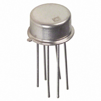
IC TRANS DUAL MATCHED NPN TO78-6
Manufacturer
Analog Devices Inc
Datasheet
1.MAT02EH.pdf
(12 pages)
Specifications of MAT02FH
Transistor Type
2 NPN (Dual)
Current - Collector (ic) (max)
20mA
Voltage - Collector Emitter Breakdown (max)
40V
Vce Saturation (max) @ Ib, Ic
200mV @ 100µA, 1mA
Current - Collector Cutoff (max)
4nA
Power - Max
1.8W
Frequency - Transition
200MHz
Mounting Type
Through Hole
Package / Case
TO-78-6 Metal Can
Lead Free Status / RoHS Status
Contains lead / RoHS non-compliant
Dc Current Gain (hfe) (min) @ Ic, Vce
-
Available stocks
Company
Part Number
Manufacturer
Quantity
Price


MAT02
more troublesome because they vary with signal levels and are
multiplied by absolute temperature. At 25°C, kT/q is
approximately 26 mV and the error due to an r
r
ing a collector current range of up to 200 µA, then a peak error
of 0.3% could be expected for an r
the MAT02. Total error is dependent on the specific application
configuration (multiply, divide, square, etc.) and the required
dynamic range. An obvious way to reduce I
duce the maximum collector current, but then op amp offsets
and leakage currents become a limiting factor at low input lev-
els. A design range of no greater than 10 µA to 1 mA is generally
recommended for most nonlinear function circuits.
A powerful technique for reducing error due to I
Figure 4. A small voltage equal to I
tor base. For this circuit:
The error from r
Since the MAT02 bulk resistance is approximately 0.39 Ω, an
R
In more complex circuits, such as the circuit in Figure 3, it may
be inconvenient to apply a compensation voltage to each indi-
vidual base. A better approach is to sum all compensation to the
bases of Q1. The “A” side needs a base voltage of (V
R
r
this compensation technique.
Operational amplifier offsets are another source of error. In
Figure 4, the input offset voltage and input bias current will
cause an error in collector current of (V
offset op amp, such as the OP07 with less than 75 µV of V
and I
micropower op amp, should be considered if low power con-
BE
BE
C
3
) r
I
. Linearity of better than ± 0.1% is readily achievable with
of 3.9 Ω and R
C
/26 mV. Using an r
BE
B
, and the “B” side needs a base voltage of (V
of less than ± 3 nA, is recommended. The OP193,
V
B
=
BE
R
R
I
2
C
C
2
of 10 R
is cancelled if R
V
1
BE
and I
of 0.4 Ω for the MAT02 and assum-
1
will give good error cancellation.
C
r
BE
=
BE
C
C
/R
r
r
I
BE
R
C
BE
2
1
error term when using
is made equal to r
is applied to the transis-
V
OS
1
C
/R
r
BE
1
BE
) + I
Figure 5. Four-Quadrant Multiplier
error is to re-
C
I
r
C
BE
O
X
term will be
/R
B
/R
. A low
is shown in
O
1
+V
+ V
OUT
Y
(10)
Z
/R
OS
/
R
2
1
)
.
–8–
sumption or single-supply operation is needed. The value of
frequency-compensating capacitor (C
op amp frequency response and peak collector current. Typi-
cal values for C
FOUR-QUADRANT MULTIPLIER
A simplified schematic for a four-quadrant log-antilog multiplier
is shown in Figure 5. Similar to the previously discussed one-
quadrant multiplier, the circuit makes I
input currents, I
This positive offset is then subtracted out at the output stage.
Assuming ideal op amps, the currents are:
From I
Figure 4. Compensation of Bulk Resistance Error
O
= I
I
O
1
=
I
I
V
2
1
R
/I
V
X
O
1
=
1
3
O
, the output voltage will be:
and I
range from 30 pF to 300 pF.
V
+
R
=
X
1
V
R
Y
R
+
1
2
R
O
, are each offset in the positive direction.
V
+
R
1
R
2
R
2
V
R
2
,
R
V
2
I
V
X
2
+
V
=
R
V
R
Y
V
O
O
R
Y
1
,
I
+
3
V
O
O
=
R
) is dependent on the
R
2
= I
V
R
R
2
1
I
2
/I
3
. The two
REV. E
(11)
(12)
Related parts for MAT02FH
Image
Part Number
Description
Manufacturer
Datasheet
Request
R

Part Number:
Description:
±1.7g Dual-Axis IMEMS Accelerometer Evaluation Board
Manufacturer:
Analog Devices Inc
Datasheet:

Part Number:
Description:
Inertial Sensor Evaluation System
Manufacturer:
Analog Devices Inc
Datasheet:
Part Number:
Description:
Manufacturer:
Analog Devices Inc
Datasheet:
Part Number:
Description:
Manufacturer:
Analog Devices Inc
Datasheet:
Part Number:
Description:
Manufacturer:
Analog Devices Inc
Datasheet:
Part Number:
Description:
Manufacturer:
Analog Devices Inc
Datasheet:
Part Number:
Description:
Manufacturer:
Analog Devices Inc
Datasheet:
Part Number:
Description:
Manufacturer:
Analog Devices Inc
Datasheet:
Part Number:
Description:
Manufacturer:
Analog Devices Inc
Datasheet:
Part Number:
Description:
Manufacturer:
Analog Devices Inc
Datasheet:
Part Number:
Description:
Manufacturer:
Analog Devices Inc
Datasheet:
Part Number:
Description:
Manufacturer:
Analog Devices Inc
Datasheet:
Part Number:
Description:
Manufacturer:
Analog Devices Inc
Datasheet: