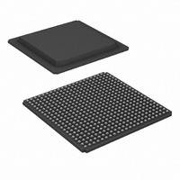
XC3S1600E-4FGG484I Xilinx Inc, XC3S1600E-4FGG484I Datasheet - Page 160

XC3S1600E-4FGG484I
Manufacturer Part Number
XC3S1600E-4FGG484I
Description
FPGA Spartan®-3E Family 1.6M Gates 33192 Cells 572MHz 90nm (CMOS) Technology 1.2V 484-Pin FBGA
Manufacturer
Xilinx Inc
Series
Spartan™-3Er
Datasheet
1.XC3S100E-4VQG100C.pdf
(233 pages)
Specifications of XC3S1600E-4FGG484I
Package
484FBGA
Family Name
Spartan®-3E
Device Logic Cells
33192
Device Logic Units
3688
Device System Gates
1600000
Number Of Registers
29504
Maximum Internal Frequency
572 MHz
Typical Operating Supply Voltage
1.2 V
Maximum Number Of User I/os
376
Ram Bits
663552
Number Of Logic Elements/cells
33192
Number Of Labs/clbs
3688
Total Ram Bits
663552
Number Of I /o
376
Number Of Gates
1600000
Voltage - Supply
1.14 V ~ 1.26 V
Mounting Type
Surface Mount
Operating Temperature
-40°C ~ 100°C
Package / Case
484-BBGA
Lead Free Status / RoHS Status
Lead free / RoHS Compliant
For Use With
HW-XA3S1600E-UNI-G - KIT DEVELOPMENT AUTOMOTIVE ECU
Lead Free Status / RoHS Status
Lead free / RoHS Compliant
Available stocks
Company
Part Number
Manufacturer
Quantity
Price
Company:
Part Number:
XC3S1600E-4FGG484I
Manufacturer:
XILINX
Quantity:
140
Company:
Part Number:
XC3S1600E-4FGG484I
Manufacturer:
XILINX
Quantity:
250
Company:
Part Number:
XC3S1600E-4FGG484I
Manufacturer:
Xilinx Inc
Quantity:
10 000
Part Number:
XC3S1600E-4FGG484I
Manufacturer:
XILINX/赛灵思
Quantity:
20 000
DC and Switching Characteristics
IEEE 1149.1/1553 JTAG Test Access Port Timing
Table 123: Timing for the JTAG Test Access Port
160
Notes:
1.
Clock-to-Output Times
T
Setup Times
T
T
Hold Times
T
T
Clock Timing
T
T
F
TCKTDO
TDITCK
TMSTCK
TCKTDI
TCKTMS
CCH
CCL
TCK
The numbers in this table are based on the operating conditions set forth in
Symbol
TCK
TMS
TDI
TDO
(Input)
(Input)
(Input)
(Output)
The time from the falling transition on the TCK pin
to data appearing at the TDO pin
The time from the setup of data at the TDI pin to
the rising transition at the TCK pin
The time from the setup of a logic level at the TMS
pin to the rising transition at the TCK pin
The time from the rising transition at the TCK pin
to the point when data is last held at the TDI pin
The time from the rising transition at the TCK pin
to the point when a logic level is last held at the
TMS pin
The High pulse width at the TCK pin
The Low pulse width at the TCK pin
Frequency of the TCK signal
Description
T
TDITCK
T
TMSTCK
Figure 79: JTAG Waveforms
www.xilinx.com
T
TCKTDI
T
TCKTMS
Table
77.
T
TCKTDO
Min
1.0
7.0
7.0
All Speed Grades
0
0
5
5
-
T
CCH
1/F
TCK
DS312-3 (v3.8) August 26, 2009
Max
11.0
30
-
-
-
-
-
-
T
CCL
Product Specification
DS312-3_79_032409
Units
MHz
ns
ns
ns
ns
ns
ns
ns
R


