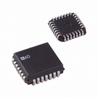
AD1671JP Analog Devices Inc, AD1671JP Datasheet - Page 8

AD1671JP
Manufacturer Part Number
AD1671JP
Description
ADC Single Pipelined 1.25MSPS 12-Bit Parallel 28-Pin PLCC
Manufacturer
Analog Devices Inc
Datasheet
1.AD1671JP.pdf
(16 pages)
Specifications of AD1671JP
Package
28PLCC
Resolution
12 Bit
Sampling Rate
1250 KSPS
Architecture
Pipelined
Number Of Analog Inputs
1
Digital Interface Type
Parallel
Input Type
Voltage
Polarity Of Input Voltage
Unipolar|Bipolar
Rohs Status
RoHS non-compliant
Number Of Bits
12
Sampling Rate (per Second)
1.25M
Data Interface
Parallel
Number Of Converters
2
Power Dissipation (max)
750mW
Voltage Supply Source
Analog and Digital, Dual ±
Operating Temperature
0°C ~ 70°C
Mounting Type
Surface Mount
Package / Case
28-LCC (J-Lead)
Lead Free Status / RoHS Status
Available stocks
Company
Part Number
Manufacturer
Quantity
Price
Part Number:
AD1671JP
Manufacturer:
ADI/亚德诺
Quantity:
20 000
Company:
Part Number:
AD1671JPZ
Manufacturer:
AD
Quantity:
1 000
AD1671
Figure 4 plots both S/(N+D) and Effective Number of Bits
(ENOB) for a 100 kHz input signal sampled from 666 kHz to
1.25 MHz.
Figure 5 is a THD plot for a full-scale 100 kHz input signal with
the sample frequency swept from 666 kHz to 1.25 MHz.
The AD1671’s SFDR performance is ideal for use in communi-
cation systems such as high speed modems and digital radios.
The SFDR is better than 84 dB with sample rates up to 1.11 MHz
and increases as the input signal amplitude is attenuated by ap-
proximately 3 dB. Note also the SFDR is typically better than
80 dB with input signals attenuated by up to –7 dB.
Figure 4. S/(N/D) vs. Sampling Frequency, f
Figure 6. Spurious Free Dynamic Range vs. Sampling
Rate, f
71.5
72.5
70.5
69.5
68.5
72
70
69
68
71
666
Figure 5. THD vs. Sampling Rate, f
–86
–68
–70
–72
–74
–76
–78
–80
–82
–84
–68
–70
–72
–74
–76
–78
–80
–82
–84
–86
–88
–90
IN
666
666
= 100 kHz
714
714
714
769
SAMPLING FREQUENCY – kHz
SAMPLING FREQUENCY – kHz
769
SAMPLING FREQUENCY – kHz
769
833
833
833
909
909
909
1000
1000
1000
IN
1111
= 100 kHz
1111
1111
IN
1250
= 100 kHz
11.50
11.25
11.75
11.00
1250
1250
–8–
APPLYING THE AD1671
GROUNDING AND DECOUPLING RULES
Proper grounding and decoupling should be a primary design
objective in any high speed, high resolution system. The
AD1671 separates analog and digital grounds to optimize the
management of analog and digital ground currents in a system.
The AD1671 is designed to minimize the current flowing from
REF COM (Pin 20) by directing the majority of the current
from V
log ground currents hence reduces the potential for large ground
voltage drops. This can be especially true in systems that do not
utilize ground planes or wide ground runs. REF COM is also
configured to be code independent, therefore reducing input de-
pendent analog ground voltage drops and errors. Code depen-
dent ground current is diverted to ACOM (Pin 27). Also critical
in any high speed digital design is the use of proper digital
grounding techniques to avoid potential CMOS “ground
bounce.” Figure 3 is provided to assist in the proper layout,
grounding and decoupling techniques.
Figure 7. Spurious Free Dynamic Range vs. Input
Amplitude, f
AGP*
V
CC
IN
Figure 8. AD1671 Grounding and Decoupling
85
80
75
70
65
60
55
50
45
40
( 5V)
–50
(+5 V–Pin 28) to V
DGP*
1 F
0.1 F
–45
IN
= 250 kHz
–40
10 F
23
22
20
27
19
25
26
24
21
*GROUND PLANE RECOMMENDED
AIN1
REF IN
REF OUT
AIN2
REF COM
ACOM
DCOM
SHA OUT
BPO/UPO
+5V
V
–35
28
CC
ANALOG INPUT – dB
0.1 F
–30
EE
AD1671
(–5 V–Pin 1). Minimizing ana-
–25
10 F
–20
–5V
V
1
EE
ENCODE
V
–15
BIT 12
+5V
LOGIC
18
BIT 1
MSB
DAV
OTR
–10
13
17
16
15
14
0.1 F
2
–5
10 F
REV. B
0


