MJE3439G ON Semiconductor, MJE3439G Datasheet
MJE3439G
Specifications of MJE3439G
Available stocks


Related parts for MJE3439G

MJE3439G Summary of contents
Page 1
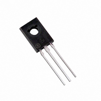
... POWER TRANSISTOR NPN SILICON 350 VOLTS, 15 WATTS TO−225 CASE 77 STYLE MARKING DIAGRAM YWW E3439G Y = Year WW = Work Week E3439 = Device Code G = Pb−Free Package ORDERING INFORMATION Device Package Shipping MJE3439 TO−225 500 Units/Box TO−225 500 Units/Box MJE3439G (Pb−Free) Publication Order Number: MJE3439/D ...
Page 2
ELECTRICAL CHARACTERISTICS Î Î Î Î Î ...
Page 3
The Safe Operating Area Curves indicate I Collector load lines for specific circuits must ...
Page 4
... American Technical Support: 800−282−9855 Toll Free USA/Canada Japan: ON Semiconductor, Japan Customer Focus Center 2−9−1 Kamimeguro, Meguro−ku, Tokyo, Japan 153−0051 Phone: 81−3−5773−3850 http://onsemi.com 4 NOTES: 1. DIMENSIONING AND TOLERANCING PER ANSI Y14.5M, 1982. 2. CONTROLLING DIMENSION: INCH. ...