Î Î Î Î Î Î Î Î Î Î Î Î Î Î Î Î Î Î Î
Î Î Î Î Î Î Î Î Î Î Î Î Î Î Î Î Î Î Î
Î Î Î Î Î Î Î Î Î Î Î Î
Î Î Î Î Î Î Î Î Î Î Î Î
Î Î Î Î Î Î Î Î Î Î Î Î
Î Î Î Î Î Î Î Î Î Î Î Î
Î Î Î Î Î Î Î Î Î Î Î Î
Î Î Î Î Î Î Î Î Î Î Î Î
Î Î Î Î Î Î Î Î Î Î Î Î
Î Î Î Î Î Î Î Î Î Î Î Î
Î Î Î Î Î Î Î Î Î Î Î Î
Î Î Î Î Î Î Î Î Î Î Î Î
Î Î Î Î Î Î Î Î Î Î Î Î
Î Î Î Î Î Î Î Î Î Î Î Î
Î Î Î Î Î Î Î Î Î Î Î Î
Î Î Î Î Î Î Î Î Î Î Î Î
Î Î Î Î Î Î Î Î Î Î Î Î
Î Î Î Î Î Î Î Î Î Î Î Î
Î Î Î Î Î Î Î Î Î Î Î Î
Î Î Î Î Î Î Î Î Î Î Î Î
Î Î Î Î Î Î Î Î Î Î Î Î
Î Î Î Î Î Î Î Î Î Î Î Î Î Î Î Î Î Î Î
Î Î Î Î Î Î Î Î Î Î Î Î Î Î Î Î Î Î Î
Î Î Î Î Î Î Î Î Î Î Î Î
Î Î Î Î Î Î Î Î Î Î Î Î
Î Î Î Î Î Î Î Î Î Î Î Î
Î Î Î Î Î Î Î Î Î Î Î Î
Î Î Î Î Î Î Î Î Î Î Î Î
Î Î Î Î Î Î Î Î Î Î Î Î
TIP3055 (NPN),
TIP2955 (PNP)
Complementary Silicon
Power Transistors
Features
•
•
•
•
Maximum ratings are those values beyond which device damage can occur.
Maximum ratings applied to the device are individual stress limit values (not
normal operating conditions) and are not valid simultaneously. If these limits are
exceeded, device functional operation is not implied, damage may occur and
reliability may be affected.
*For additional information on our Pb−Free strategy and soldering details, please
MAXIMUM RATINGS
THERMAL CHARACTERISTICS
© Semiconductor Components Industries, LLC, 2005
September, 2005 − Rev. 6
download the ON Semiconductor Soldering and Mounting Techniques
Reference Manual, SOLDERRM/D.
Collector − Emitter Voltage
Collector − Emitter Voltage
Collector − Base Voltage
Emitter − Base Voltage
Collector Current − Continuous
Base Current
Total Power Dissipation @ T
Derate above 25_C
Operating and Storage Junction
Temperature Range
Thermal Resistance, Junction−to−Case
Thermal Resistance, Junction−to−Ambient
Designed for general−purpose switching and amplifier applications.
DC Current Gain −
Collector−Emitter Saturation Voltage −
Excellent Safe Operating Area
Pb−Free Packages are Available*
h
V
FE
Characteristic
CE(sat)
= 20−70 @ I
= 4.0 Adc
Rating
= 1.1 Vdc (Max) @ I
= 4.0 Adc
C
= 25_C
C
Î Î Î
Î Î Î
Î Î Î
Î Î Î
Î Î Î
Î Î Î
Î Î Î
Î Î Î
Î Î Î
Î Î Î
Î Î Î
Î Î Î
Î Î Î
Î Î Î
Î Î Î
Î Î Î
Î Î Î
Î Î Î
Î Î Î
Î Î Î
Î Î Î
Î Î Î
Î Î Î
Î Î Î
Î Î Î
Symbol
Symbol
T
C
V
V
R
R
J
V
V
P
, T
CEO
CER
I
I
qJC
qJA
CB
EB
C
B
D
stg
Î Î Î Î
Î Î Î Î
Î Î Î Î
Î Î Î Î
Î Î Î Î
Î Î Î Î
Î Î Î Î
Î Î Î Î
Î Î Î Î
Î Î Î Î
Î Î Î Î
Î Î Î Î
Î Î Î Î
Î Î Î Î
Î Î Î Î
Î Î Î Î
Î Î Î Î
Î Î Î Î
Î Î Î Î
Î Î Î Î
Î Î Î Î
Î Î Î Î
Î Î Î Î
Î Î Î Î
Î Î Î Î
– 65 to
Value
+ 150
0.72
Max
1.39
35.7
100
7.0
1 5
7.0
60
70
90
Î Î Î
Î Î Î
Î Î Î
Î Î Î
Î Î Î
Î Î Î
Î Î Î
Î Î Î
Î Î Î
Î Î Î
Î Î Î
Î Î Î
Î Î Î
Î Î Î
Î Î Î
Î Î Î
Î Î Î
Î Î Î
Î Î Î
Î Î Î
Î Î Î
Î Î Î
Î Î Î
Î Î Î
Î Î Î
1
W/_C
_C/W
_C/W
Unit
Unit
Vdc
Vdc
Vdc
Vdc
Adc
Adc
_C
W
See detailed ordering and shipping information in the package
dimensions section on page 2 of this data sheet.
COMPLEMENTARY SILICON
POWER TRANSISTORS
60 VOLTS, 90 WATTS
A
Y
WW
TIPxx55
xx
G
ORDERING INFORMATION
MARKING DIAGRAM
http://onsemi.com
15 AMPERE
= Assembly Location
= Year
= Work Week
= Device Code
= 30 or 29
= Pb−Free Package
AYWWG
TIPxx55
Publication Order Number:
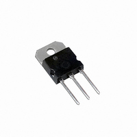
SOT−93 (TO−218)
CASE 340D
STYLE 1
TIP3055/D