MJ11033G ON Semiconductor, MJ11033G Datasheet
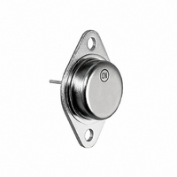
TRANS DARL PNP 50A 120V TO3

MJ11033G

Manufacturer Part Number
MJ11033G
Description
TRANS DARL PNP 50A 120V TO3
Manufacturer
ON Semiconductor
Type
High Current, Powerr
Datasheets

Specifications of MJ11033G

Transistor Type
PNP - Darlington
Current - Collector (ic) (max)
50A
Voltage - Collector Emitter Breakdown (max)
120V
Vce Saturation (max) @ Ib, Ic
3.5V @ 500mA, 50A
Current - Collector Cutoff (max)
2mA
Dc Current Gain (hfe) (min) @ Ic, Vce
1000 @ 25A, 5V
Power - Max
300W
Mounting Type
Chassis Mount
Package / Case
TO-204, TO-3
Configuration
Single
Transistor Polarity
PNP
Mounting Style
Through Hole
Collector- Emitter Voltage Vceo Max
120 V
Emitter- Base Voltage Vebo
5 V
Collector- Base Voltage Vcbo
120 V
Maximum Dc Collector Current
50 A
Power Dissipation
0.3 W
Maximum Operating Temperature
+ 200 C
Continuous Collector Current
50 A
Dc Collector/base Gain Hfe Min
400, 1000
Minimum Operating Temperature
- 55 C
Current, Gain
400
Current, Input
2 A
Current, Output
50 A
Current, Output, Leakage
2
Package Type
TO-204 (TO-3)
Polarity
PNP
Primary Type
Si
Voltage, Collector To Emitter, Saturation
3.5 V
Voltage, Input
5 V
Voltage, Output
120 V
Lead Free Status / RoHS Status
Lead free / RoHS Compliant
Frequency - Transition
-
Lead Free Status / Rohs Status
Lead free / RoHS Compliant
Other names
MJ11033GOS

Available stocks

Company
Part Number
Manufacturer
Quantity
Price
Part Number:
MJ11033G
Manufacturer:
ON
Quantity:
2 000
Part Number:
MJ11033G
Manufacturer:
NUVOTON
Quantity:
20 000
Company:
Part Number:
MJ11033G
Quantity:
1 008
Î Î Î Î Î Î Î Î Î Î Î Î
MJ11028, MJ11030,
MJ11032 (NPN)
MJ11029, MJ11033 (PNP)
High-Current
Complementary Silicon
Power Transistors
as output devices in complementary general purpose amplifier
applications.
Features
Maximum ratings are those values beyond which device damage can occur.
Maximum ratings applied to the device are individual stress limit values (not
normal operating conditions) and are not valid simultaneously. If these limits are
exceeded, device functional operation is not implied, damage may occur and
reliability may be affected.
1. Pulse Test: Pulse Width = 5 ms, Duty Cycle ≤ 10%.
*For additional information on our Pb−Free strategy and soldering details, please
© Semiconductor Components Industries, LLC, 2008
September, 2008 − Rev. 6
MAXIMUM RATINGS
THERMAL CHARACTERISTICS
download the ON Semiconductor Soldering and Mounting Techniques
Reference Manual, SOLDERRM/D.
Collector−Emitter Voltage
Collector−Base Voltage
Emitter−Base Voltage
Base Current − Continuous
Total Power Dissipation @ T
Derate Above 25°C @ T
Operating and Storage Junction
Temperature Range
Maximum Lead Temperature for
Soldering Purposes for v 10 seconds
Thermal Resistance, Junction−to−Case
Collector Current − Continuous
High−Current Complementary Silicon Power Transistors are for use
High DC Current Gain − h
Curves to 100 A (Pulsed)
Diode Protection to Rated I
Monolithic Construction with Built−In Base−Emitter Shunt Resistor
Junction Temperature to + 200_C
Pb−Free Packages are Available*
Characteristic
Rating
− Peak (Note 1)
C
(T
= 100_C
J
C
= 25°C unless otherwise noted)
= 25°C
h
MJ11028/29
MJ11032/33
MJ11028/29
MJ11032/33
FE
FE
C
MJ11030
MJ11030
= 1000 (Min) @ I
= 400 (Min) @ I
Î Î Î
Î Î Î
Î Î Î
Symbol
Symbol
T
V
V
V
R
J
P
CEO
CBO
EBO
, T
T
I
I
qJC
C
B
D
L
stg
Î Î Î Î Î
Î Î Î Î Î
Î Î Î Î Î
C
C
= 50 Adc
− 55 to +200
= 25 Adc
Value
1.71
Max
0.58
120
120
100
300
275
5.0
2.0
60
90
60
90
50
1
Î Î
Î Î
Î Î
W/°C
°C/W
Unit
Unit
Vdc
Vdc
Vdc
Adc
Adc
_C
°C
W
See detailed ordering and shipping information in the package
dimensions section on page 3 of this data sheet.
BASE
1
TO−204 (TO−3)
MJ110xx = Device Code
G
A
YY
WW
MEX
DARLINGTON POWER
CASE 197A
ORDERING INFORMATION
STYLE 1
COMPLEMENTARY
COLLECTOR
CASE
EMITTER 2
2
MJ11028
MJ11030
MJ11032
60 − 120 VOLTS
TRANSISTORS
NPN
http://onsemi.com
1
50 AMPERE
300 WATTS
= Pb−Free Package
= Location Code
= Year
= Work Week
= Country of Orgin
xx = 28, 29, 30, 32, 33
Publication Order Number:
BASE
1
MARKING
DIAGRAM
MJ110xxG
AYYWW
COLLECTOR
CASE
MEX
EMITTER 2
MJ11029
MJ11033
PNP
MJ11028/D

Related parts for MJ11033G

MJ11033G Summary of contents

Page 1

... Pulse Test: Pulse Width = 5 ms, Duty Cycle ≤ 10%. *For additional information on our Pb−Free strategy and soldering details, please download the ON Semiconductor Soldering and Mounting Techniques Reference Manual, SOLDERRM/D. © Semiconductor Components Industries, LLC, 2008 September, 2008 − Rev. 6 ...

Page 2

PNP MJ11029 MJ11033 BASE ≈ 3.0 k ELECTRICAL CHARACTERISTICS Characteristic OFF CHARACTERISTICS Collector−Emitter Breakdown Voltage (Note mAdc Collector−Emitter Leakage Current ( Vdc kW ...

Page 3

... ORDERING INFORMATION Device MJ11028 MJ11028G MJ11029 MJ11029G MJ11030 MJ11030G MJ11032 MJ11032G MJ11033 MJ11033G 100 BONDING WIRE LIMITED THERMALLY LIMITED @ T = 25° SECOND BREAKDOWN LIMITED 1 MJ11028, 29 0.5 MJ11032, 33 0.2 0.1 0.2 0 COLLECTOR-EMITTER VOLTAGE (VOLTS) CE Figure 2. DC Safe Operating Area 100 25° MJ11029, MJ11033 PNP ...

Page 4

... Opportunity/Affirmative Action Employer. This literature is subject to all applicable copyright laws and is not for resale in any manner. PUBLICATION ORDERING INFORMATION LITERATURE FULFILLMENT: Literature Distribution Center for ON Semiconductor P.O. Box 5163, Denver, Colorado 80217 USA Phone: 303−675−2175 or 800−344−3860 Toll Free USA/Canada Fax: 303− ...

Related keywords