AX5151-TSSOP24-TU AXSEM, AX5151-TSSOP24-TU Datasheet
AX5151-TSSOP24-TU
Specifications of AX5151-TSSOP24-TU


Related parts for AX5151-TSSOP24-TU


AX5151-TSSOP24-TU Summary of contents
Page 1
... DATASHEET AX5151 Version 1.0 ...
Page 2
... Document Type Datasheet Document Status Document Version Version 1.0 Product AX5151 Version 1.0 Datasheet AX5151 ...
Page 3
... RF Frequency Generation Subsystem (Synthesizer) ................................................................ 14 Transmitter...................................................................................................................................... 15 Receiver ......................................................................................................................................... 16 SPI Timing........................................................................................................................................ 18 5. Circuit Description ................................................................................................................... 19 5.1. Voltage Regulator ....................................................................................................................... 20 5.2. Crystal Oscillator........................................................................................................................... 20 5.3. SYSCLK Output.............................................................................................................................. 21 5.4. Power-on-reset (POR) and RESET_N Input ................................................................................ 21 5.5. RF Frequency Generation Subsystem....................................................................................... 21 VCO ................................................................................................................................................ 22 VCO Auto-Ranging ...................................................................................................................... 22 Loop Filter and Charge Pump .................................................................................................... 22 Version 1.0 3 Table of Contents Datasheet AX5151 ...
Page 4
... PWRMODE Register ................................................................................................................ 29 5.15. Serial Peripheral Interface (SPI) ............................................................................................ 31 SPI Timing........................................................................................................................................ 31 6. Register Bank Description ....................................................................................................... 32 6.1. Control Register Map................................................................................................................... 33 7. Application Information.......................................................................................................... 37 7.1. Typical Application Diagram ..................................................................................................... 37 7.2. Antenna Interface Circuitry........................................................................................................ 38 Single-Ended Antenna Interface ............................................................................................... 38 Dipole Antenna Interface ........................................................................................................... 39 7.3. Voltage Regulator ....................................................................................................................... 39 Version 1.0 Datasheet AX5151 ...
Page 5
... TSSOP24 Package Information ............................................................................................... 40 8.1. Package Outline TSSOP24 .......................................................................................................... 40 9. Life Support Applications ........................................................................................................ 42 10. Contact Information ................................................................................................................ 43 Version 1.0 5 Table of Contents Datasheet AX5151 ...
Page 6
... Toys • Wireless audio • Wireless networks • Wireless USB • Access control • Remote keyless entry • ARIB compatible • Pointing devices and keyboards • Active RFID • RFID base station transmitter • 433/868/915 MHz SRD band systems Datasheet AX5151 ...
Page 7
... AGC PGAs ANTP 4 5 ANTN PA F OUT Crystal Oscillator RF Frequency F XTAL typ. Generation 16 MHz Subsystem Divider Figure 1 Functional block diagram of the AX5151 Version 1.0 AX5151 Digital IF De- ADC channel modulator filter RSSI AGC Modulator Communication Controller & Chip configuration Voltage POR Regulator ...
Page 8
... Can be programmed to be used as a general purpose I/O pin P Unregulated power supply P Ground P Ground Regulated output voltage P VDD pins must be connected to this supply voltage A 1µF low ESR capacitor to GND must be connected to this pin I/O = digital input/output signal N = not to be connected P = power or ground Datasheet AX5151 ...
Page 9
... Pinout Drawing 1 NC CLK16P 2 CLK16N 3 4 GND VDD 5 GND 6 7 ANT1 ANT2 8 GND 9 VDD 10 GND 11 GND 12 Version 1.0 VREG 24 GND 23 GND 22 VDD_IO 21 IRQ 20 TST 19 AX5151 MOSI 18 MISO 17 CLK 16 SEL_n 15 SYSCLK 14 RESET_N 13 Figure 2: Pinout drawing (Top view) 9 Pin Function Descriptions Datasheet AX5151 ...
Page 10
... Electrostatic handling es T Operating temperature amb T Storage temperature stg T Junction Temperature j Version 1.0 CONDITION MIN -0.5 -10 -100 -0.5 -0.5 HBM -2000 -20 -65 MAX UNIT 5.5 V 100 mA 800 mW 15 dBm 10 mA 100 5.5 V 5.5 V 2000 V 70 °C 150 °C 150 °C Datasheet AX5151 ...
Page 11
... MHz, 10 dBm 868 MHz, 4 dBm 868 MHz, 0 dBm 868 MHz, -12 dBm 433 MHz, 12 dBm 433 MHz, 6dBm 433 MHz, 2 dBm 433 MHz, -8 dBm 11 Specifications TYP. MAX. UNIT 27 70 °C 3.0 3.6 V 3.0 3.6 V 1.7 V 2.5 2 300 mV 0.5 µ Datasheet AX5151 ...
Page 12
... Input voltage, low IL V Input voltage, high IH I Input leakage current L DIGITAL OUTPUTS I Output Current, high OH I Output Current, low OL I Tri-state output leakage current OZ Version 1.0 CONDITION MIN. TYP. 1.9 1.2 2 -10 MAX. UNIT µ µA Datasheet AX5151 ...
Page 13
... XTALOSCGM =0101 6 XTALOSCGM =0110 6.5 XTALOSCGM =0111 7 XTALOSCGM =1000 7.5 XTALOSCGM =1001 8 XTALOSCGM =1010 8.5 XTALOSCGM =1011 9 XTALOSCGM =1100 9.5 XTALOSCGM =1101 10 XTALOSCGM =1110 10.5 XTALOSCGM =1111 11 XTALCAP = 000000 2 default XTALCAP = 111111 33 0.5 Note Specifications MAX. UNIT MHz MHz kΩ Datasheet AX5151 ...
Page 14
... MHz, 300 kHz from carrier 433 MHz, 2 MHz from carrier TYP. MAX. UNIT 16 MHz 930 MHz 470 Hz 100 50 kHz 200 500 15 30 µ µ -85 -90 -100 -110 dBc/Hz -90 -95 -105 -115 -80 -90 -105 -115 dBc/Hz -90 -95 -110 -122 Datasheet AX5151 ...
Page 15
... TXRNG=0001 -9.5 TXRNG=0010 -4 TXRNG=0011 -0.5 TXRNG=0100 1.5 TXRNG=0101 3.5 TXRNG=0110 4.5 TXRNG=0111 5.5 TXRNG=1000 6.5 TXRNG=1001 7.5 TXRNG=1010 8 TXRNG=1011 8.5 TXRNG=1100 9 TXRNG=1101 9.5 TXRNG=1110 10 TXRNG=1111 10.5 TXRNG=1111 11 -50 Note 1 -55 15 Specifications MAX. UNIT 600 kbps 200 -40 dBm dBm dBc Datasheet AX5151 ...
Page 16
... AGCCOUNTER Behind digital channel filter; calculated from registers AGCCOUNTER, TRKAMPL MIN. TYP. MAX. UNIT 38.4 600 kbps 38.4 200 -101 -100 -98 -95 -102 -101 dBm -99 -97 -98 -95 -93 -100 -99 -98 -96 -93 -100 -99 dBm -97 -93 -96 -93 -91 -98 -20 dBm -35 dBm - 0.625 dB 0.1 dB Datasheet AX5151 ...
Page 17
... Sensitivities for the 433 MHz band are 1-2 dB better than those for the 868 MHz band Version 1.0 CONDITION MIN. TYP. FSK 50 kbps, notes 1 & 2 FSK 100 kbps, notes 1 & 3 PSK 200 kbps, notes 1 & 4 FSK 100 kbps, note 5 17 Specifications MAX. UNIT Datasheet AX5151 ...
Page 18
... CLK low duration Tch CLK high duration Notes 1. For SPI access during power-down mode the period should be relaxed to 100ns. For a figure showing the SPI timing parameters see section 5.15: Serial Peripheral Interface (SPI). Version 1.0 CONDITION MIN. TYP Note MAX. UNIT Datasheet AX5151 ...
Page 19
... The AX5151 behaves as a SPI slave interface. Configuration of the AX5151 is also done via the SPI interface. AX5151 supports any data rate from 38.4 kbps to 200 kbps for FSK and MSK and from 38.4 kbps for 600 kbps for ASK and PSK. To achieve optimum performance for specific data rates and modulation schemes several register settings to configure the AX5151 are necessary, they are outlined in the following, for details see the AX5151 Programming Manual ...
Page 20
... Voltage Regulator The AX5151 uses an on-chip voltage regulator to create a stable supply voltage for the internal circuitry at pin VREG from the primary supply VDD_IO. All VDD pins of the device must be connected to VREG. The antenna pins ANTP and ANTN must be DC biased to VREG. The I/O level of the digital pins is VDD_IO. The voltage regulator requires a 1µ ...
Page 21
... PCB to avoid interference. 5.4. Power-on-reset (POR) and RESET_N Input AX5151 has an integrated power-on-reset block. No external POR circuit or signal at the RESET_N pin is required, prior to POR the RESET_N pin is disabled. After POR the AX5151 can be reset in two ways SPI accesses: the bit RST in the PWRMODE register is toggled. ...
Page 22
... MHz band, the BANDSEL bit in the PLLLOOP register must be programmed. VCO Auto-Ranging The AX5151 has an integrated auto-ranging function, which allows to set the correct VCO range for specific frequency generation subsystem settings automatically. Typically it has to be executed after power-up. The function is initiated by setting the RNG_START bit in the PLLRANGING register ...
Page 23
... The channel filter offers bandwidths of 40 kHz up to 600 kHz. For detailed instructions how to program the digital channel filter and the demodulator see the AX5151 Programming Manual, an overview of the registers involved is given in the following table. The register setups typically must be done once at power-up of the device. ...
Page 24
... It does so without adding additional bits, i.e. without changing the data rate. Spectral Shaping uses a self synchronizing feedback shift register. The encoder is programmed using the register ENCODING, details and recommendations on usage are given in the AX5151 Programming Manual. Version 1.0 Remarks This register programs the bandwidth of the digital channel filter ...
Page 25
... FIFO needs servicing. In interrupt mode EMPTY, NOT EMPTY, FULL, NOT FULL and programmable level interrupts are provided. The AX5151 signals interrupts by asserting (driving high) its IRQ line. The interrupt line is level triggered, active high. Interrupts are acknowledged by removing the cause for the interrupt, i ...
Page 26
... HDLC Mode Note: HDLC mode follows High-Level Data Link Control (HDLC, ISO 13239) protocol. HDLC Mode is the main framing mode of the AX5151. In this mode, the AX5151 performs automatic packet delimiting, and optional packet correctness check by inserting and checking a cyclic redundancy check (CRC) field. ...
Page 27
... The despreader function of the receiver undoes that. In 802.15.4 mode, the AX5151 framing unit performs the spreading and despreading function according to the 802.15.4 specification. In receive mode, the framing unit will also automatically search for the 802 ...
Page 28
... TRKFREQ ∆ BITRATE 16 2 FSKMUL is the FSK oversampling factor, it depends on the FSK bit rate and deviation used. To determine it for a specific case, see the AX5151 Programming Manual. For modulations other than FSK, FSKMUL=1. Version 1.0 Bit = 1 Main Lobe Bandwidth PA on BW=BITRATE ∆f=+f BW=(1+h) ⋅ ...
Page 29
... Synthesizer and transmitter are running. Do not switch into this mode before the synthesizer has completely settled on the transmit 1101 FULLTX frequency (in SYNTHTX mode), otherwise spurious spectral transmissions will occur. Version 1.0 29 Circuit Description Typical Idd 0.5 µA 200 µA 650 µ Datasheet AX5151 ...
Page 30
... A typical PWRMODE sequence for a receive session : Step PWRMODE[3:0] Remarks 1 POWERDOWN 2 STANDBY The settling time is dominated by the crystal used, typical value 3ms The synthesizer settling time is 5 – 50 µs depending on settings, see section AC 3 SYNTHRX Characteristics 4 FULLRX Data reception 5 POWERDOWN Version 1.0 Datasheet AX5151 ...
Page 31
... Serial Peripheral Interface (SPI) The AX5151 can be programmed via a four wire serial interface according SPI using the pins CLK, MOSI, MISO and SEL. Registers for setting up the AX5151 are programmed via the serial peripheral interface in all device modes. When the interface signal SEL is pulled low bit configuration data stream is expected on the input signal pin MOSI, which is interpreted as D0 ...
Page 32
... No checks are made whether the programmed combination of bits makes sense! Bit 0 is always the LSB. Note Whole registers or register bits marked as reserved should be kept at their default values. Note All addresses not documented here must not be accessed, neither in reading nor in writing. Version 1.0 Datasheet AX5151 ...
Page 33
... Silicon Revision Scratch Register PWRMODE(3:0) Power Mode XTALOSCGM(3: Crystal Oscillator FIFO EMPTY FIFOCMD(1:0) FIFO Control FIFO Data IRQ Mask IRQ Request Interface Mode IFMODE(3:0) Must be set to 0000 SYSCLK(3:0) Pin Configuration 1 Pin Configuration 2 reserved IRQI reserved TST_PINS(1:0) must be set to 11 Datasheet AX5151 33 ...
Page 34
... CRC Initialization Data or Preamble SSREG SDS SREG Voltage Regulator Status Synthesizer Frequency Synthesizer Frequency Synthesizer Frequency Synthesizer Frequency FSK Frequency Deviation FSK Frequency Deviation FSK Frequency Deviation 2nd Frequency 2nd Frequency FLT(1:0) Synthesizer Loop Filter Settings VCOR(3:0) Synthesizer VCO Auto-Ranging Datasheet AX5151 ...
Page 35
... AGC Attack AGCDECAY(4:0) AGC Decay AGC Current Value CICSHIFT(4:0) CIC Shift Factor CIC Decimation Factor Datarate Datarate Timing Gain Timing Gain PHASEGAIN(3:0) Phase Gain FREQGAIN(3:0) Frequency Gain FREQGAIN2(3:0) Frequency Gain 2 AMPLGAIN(3:0) Amplitude Gain Amplitude Tracking Amplitude Tracking TRKPHASE(11:8) Phase Tracking Datasheet AX5151 35 ...
Page 36
... TRKFREQ(15:8) TRKFREQ(7: XTALCAP(5: reserved LOCURST reserved - - reserved - - reserved Phase Tracking Frequency Tracking Frequency Tracking Crystal oscillator tuning capacitance Synthesizer VCO current VCO_I[2:0] Must be set to 001 LOCURST Must be set to 1 REF_I[2:0] Reference adjust Misc RF settings RXIMIX(1:0) RXIMIX(1:0) must be set to 01 Datasheet AX5151 ...
Page 37
... VDD and VDD_IO pin. In order to reduce noise on the antenna inputs it is recommended to add the VDD pins close to the antenna interface. Version 1.0 1µF NC VDD VDD_IO GND AX5151 ANTP ANTN GND VDD Figure 4 Typical application diagram 37 Application Information NC IRQ TST3 MOSI MISO CLK Datasheet AX5151 ...
Page 38
... Antenna Interface Circuitry The ANTP and ANTN pins provide RF input to the LNA when AX5151 is in receive mode, and RF output from the PA when AX5151 is in transmit mode. A small antenna can be connected with an optional translation network. The network must provide DC power to the PA and LNA ...
Page 39
... Frequency L1=L2 Band [nH] 868 / 915 MHz 433 MHz 7.3. Voltage Regulator The AX5151 has an integrated voltage regulator which generates a stable supply voltage VREG from the voltage applied at VDD_IO. Use VREG to supply all the VDD supply pins. Version 1.0 L3 dipole C1 C2 antenna ...
Page 40
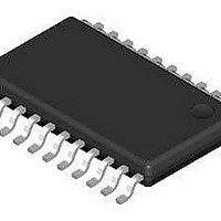
... TSSOP24 Package Information 8. TSSOP24 Package Information 8.1. Package Outline TSSOP24 Version 1.0 Datasheet AX5151 ...
Page 41
... Version 1.0 TSSOP24 Package Information Datasheet AX5151 41 ...
Page 42
... This product is not designed for use in life support appliances, devices systems where malfunction of this product can reasonably be expected to result in personal injury. AXSEM customers using or selling this product for use in such applications their own risk and agree to fully indemnify AXSEM for any damages resulting from such improper use or sale. Version 1.0 Datasheet AX5151 ...
Page 43
... Offenders will be held liable for the payment of damages. All rights reserved. Copyright © 2007 AXSEM AG Version 1.0 Contact Information Phone +41 44 882 17 07 Fax +41 44 882 17 09 Email sales@axsem.com www.axsem.com Datasheet AX5151 43 ...