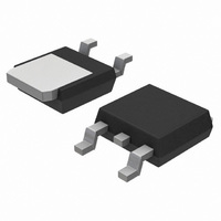
MJD117RLG ON Semiconductor, MJD117RLG Datasheet - Page 3

MJD117RLG
Manufacturer Part Number
MJD117RLG
Description
TRANS DARL PNP 2A 100V DPAK-4
Manufacturer
ON Semiconductor
Datasheet
1.MJD117T4G.pdf
(8 pages)
Specifications of MJD117RLG
Transistor Type
PNP - Darlington
Current - Collector (ic) (max)
2A
Voltage - Collector Emitter Breakdown (max)
100V
Vce Saturation (max) @ Ib, Ic
3V @ 40mA, 4A
Current - Collector Cutoff (max)
20µA
Dc Current Gain (hfe) (min) @ Ic, Vce
1000 @ 2A, 3V
Power - Max
1.75W
Frequency - Transition
25MHz
Mounting Type
Surface Mount
Package / Case
DPak, TO-252 (2 leads+tab), SC-63
Lead Free Status / RoHS Status
Lead free / RoHS Compliant
Available stocks
Company
Part Number
Manufacturer
Quantity
Price
Company:
Part Number:
MJD117RLG
Manufacturer:
ON
Quantity:
12 500
a transistor: average junction temperature and second
breakdown. Safe operating area curves indicate I
limits of the transistor that must be observed for reliable
operation; i.e., the transistor must not be subjected to greater
dissipation than the curves indicate.
is variable depending on conditions. Second breakdown
pulse limits are valid for duty cycles to 10% provided
T
Figure 4. At high case temperatures, thermal limitations will
reduce the power that can be handled to values less than the
limitations imposed by second breakdown.
J(pk)
There are two limitations on the power handling ability of
The data of Figures 5 and 6 is based on T
0.07
0.05
0.03
0.02
0.01
0.7
0.5
0.3
0.2
0.1
0.7
0.5
0.3
0.2
0.1
10
< 150_C. T
7
5
3
2
1
1
0.01
2
SINGLE PULSE
Figure 4. Maximum Rated Forward Biased
0.01
3
0.02 0.03 0.05
D = 0.5
T
CURVES APPLY BELOW RATED V
V
0.05
J
CE
0.1
= 150°C
0.2
5
J(pk)
, COLLECTOR-EMITTER VOLTAGE (VOLTS)
BONDING WIRE LIMITED
THERMAL LIMIT
SECOND BREAKDOWN LIMIT
1 ms
7
may be calculated from the data in
Safe Operating Area
10
0.1
20
dc
5 ms
0.2 0.3
30
ACTIVE−REGION SAFE−OPERATING AREA
CEO
500 ms
J(pk)
50 70
= 150_C; T
0.5
100 ms
Figure 3. Thermal Response
C
100
http://onsemi.com
− V
1
t, TIME OR PULSE WIDTH (ms)
CE
C
200
2
3
R
R
D CURVES APPLY FOR POWER
PULSE TRAIN SHOWN
READ TIME AT t
T
3
2.5
1.5
0.5
T
J(pk)
qJC(t)
qJC
A
2
1
0
200
100
= 6.25°C/W
70
50
30
20
10
- T
T
25
20
15
10
0.04
= r(t) R
5
5
0
C
25
C
= P
0.06
qJC
(pk)
10
1
0.1
q
JC(t)
50
0.2
20
PNP
NPN
SURFACE
Figure 5. Power Derating
V
MOUNT
R
Figure 6. Capacitance
T
, REVERSE VOLTAGE (VOLTS)
30
A
0.4
T, TEMPERATURE (°C)
0.6
75
50
P
(pk)
1
T
DUTY CYCLE, D = t
C
100
t
1
C
2
ib
100
t
2
200 300
4
6
T
1
C
/t
125
10
2
= 25°C
500
C
ob
20
1000
40
15


