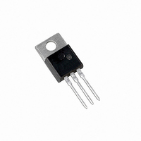
BUX85 ON Semiconductor, BUX85 Datasheet

BUX85
Manufacturer Part Number
BUX85
Description
TRANS NPN 2A 450V 50W TO220AB
Manufacturer
ON Semiconductor
Datasheet
1.BUX85G.pdf
(4 pages)
Specifications of BUX85
Transistor Type
NPN
Current - Collector (ic) (max)
2A
Voltage - Collector Emitter Breakdown (max)
450V
Vce Saturation (max) @ Ib, Ic
1V @ 200mA, 1A
Current - Collector Cutoff (max)
200µA
Dc Current Gain (hfe) (min) @ Ic, Vce
30 @ 100mA, 5V
Power - Max
50W
Frequency - Transition
4MHz
Mounting Type
Through Hole
Package / Case
TO-220-3 (Straight Leads)
Lead Free Status / RoHS Status
Contains lead / RoHS non-compliant
Other names
BUX85OS
Available stocks
Company
Part Number
Manufacturer
Quantity
Price
Company:
Part Number:
BUX85
Manufacturer:
KODENSHI
Quantity:
2 233
Part Number:
BUX85
Manufacturer:
ST
Quantity:
20 000
Part Number:
BUX85G
Manufacturer:
ON/安森美
Quantity:
20 000
BUX85G
SWITCHMODEtNPN Silicon
Power Transistors
switching applications like converters, inverters, switching regulators,
motor control systems.
Features
•
•
•
•
•
Stresses exceeding Maximum Ratings may damage the device. Maximum
Ratings are stress ratings only. Functional operation above the Recommended
Operating Conditions is not implied. Extended exposure to stresses above the
Recommended Operating Conditions may affect device reliability.
1. Pulse Test: Pulse Width = 5 ms, Duty Cycle x 10%.
*For additional information on our Pb−Free strategy and soldering details, please
MAXIMUM RATINGS
THERMAL CHARACTERISTICS
© Semiconductor Components Industries, LLC, 2010
April, 2010 − Rev. 13
download the ON Semiconductor Soldering and Mounting Techniques
Reference Manual, SOLDERRM/D.
Collector−Emitter Voltage
Collector−Emitter Voltage
Emitter−Base Voltage
Collector Current
Base Current
Reverse Base Current − Peak
Total Device Dissipation @ T
Derate above 25°C
Operating and Storage Junction
Temperature Range
Thermal Resistance, Junction−to−Case
Thermal Resistance, Junction−to−Ambient
Maximum Lead Temperature for Soldering
Purposes 1/8″ from Case for 5 Seconds
The BUX85G is designed for high voltage, high speed power
V
V
Fall time = 0.3 ms (typ) at I
V
These Devices are Pb−Free and are RoHS Compliant*
CEO(sus)
CES(sus)
CE(sat)
= 1.0 V (max) at I
Characteristics
− 1000 V
− 450 V
Rating
− Continuous
− Peak (Note 1)
− Continuous
− Peak (Note 1)
C
= 25_C
C
C
= 1.0 A, I
= 1.0 A
V
B
Symbol
Symbol
T
CEO(sus)
V
V
R
R
J
= 0.2 A
I
I
I
P
EBO
, T
T
CES
CM
BM
BM
I
I
qJC
qJA
C
B
D
L
stg
−65 to +150
Value
1000
0.75
Max
62.5
450
400
275
3.0
1.0
2.5
50
5
2
1
1
W/_C
_C/W
_C/W
Unit
Unit
Vdc
Vdc
Vdc
Adc
Adc
Adc
_C
_C
W
BUX85G
Device
POWER TRANSISTOR
450 VOLTS, 50 WATTS
1
BUX85
A
Y
WW
G
ORDERING INFORMATION
2
3
MARKING DIAGRAM
2.0 AMPERES
http://onsemi.com
NPN SILICON
(Pb−Free)
Package
TO−220
= Device Code
= Assembly Location
= Year
= Work Week
= Pb−Free Package
BUX85G
AY WW
CASE 221A−09
Publication Order Number:
TO−220AB
STYLE 1
50 Units / Rail
Shipping
BUX85/D
Related parts for BUX85
BUX85 Summary of contents
Page 1
... BUX85G SWITCHMODEtNPN Silicon Power Transistors The BUX85G is designed for high voltage, high speed power switching applications like converters, inverters, switching regulators, motor control systems. Features • V − 450 V CEO(sus) • V − 1000 V CES(sus) • Fall time = 0.3 ms (typ 1 • 1.0 V (max ...
Page 2
ELECTRICAL CHARACTERISTICS Î Î Î Î Î ...
Page 3
100 Figure 1. Test Circuit for WAVEFORM ...
Page 4
... S 0.045 0.055 1.15 1.39 T 0.235 0.255 5.97 6.47 U 0.000 0.050 0.00 1.27 V 0.045 --- 1.15 --- Z --- 0.080 --- 2.04 PIN 1. BASE 2. COLLECTOR 3. EMITTER 4. COLLECTOR ON Semiconductor Website: www.onsemi.com Order Literature: http://www.onsemi.com/orderlit For additional information, please contact your local Sales Representative BUX85/D ...


