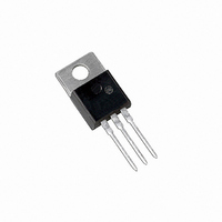
BUL146 ON Semiconductor, BUL146 Datasheet - Page 6

BUL146
Manufacturer Part Number
BUL146
Description
TRANS NPN SW 400V 8A TO-220AB
Manufacturer
ON Semiconductor
Series
SWITCHMODE™r
Datasheet
1.BUL146FG.pdf
(11 pages)
Specifications of BUL146
Transistor Type
NPN
Current - Collector (ic) (max)
6A
Voltage - Collector Emitter Breakdown (max)
400V
Vce Saturation (max) @ Ib, Ic
700mV @ 600mA, 3A
Current - Collector Cutoff (max)
100µA
Dc Current Gain (hfe) (min) @ Ic, Vce
14 @ 500mA, 5V
Power - Max
100W
Frequency - Transition
14MHz
Mounting Type
Through Hole
Package / Case
TO-220-3 (Straight Leads)
Lead Free Status / RoHS Status
Contains lead / RoHS non-compliant
Available stocks
Company
Part Number
Manufacturer
Quantity
Price
Company:
Part Number:
BUL146F
Manufacturer:
MOT
Quantity:
1 218
0.01
130
120
100
100
110
0.1
1,0
0,8
0,6
0,4
0,2
0,0
90
80
70
60
10
1
10
20
3
DC (BUL146)
Figure 15. Forward Bias Safe Operating Area
Figure 17. Forward Bias Power Derating
I
C
4
= 3 A
5 ms
40
V
CE
5
T
T
Figure 13. Inductive Fall Time
, COLLECTOR-EMITTER VOLTAGE (VOLTS)
J
J
= 25°C
= 125°C
1 ms
T
6
C
60
, CASE TEMPERATURE (°C)
7
THERMAL DERATING
h
FE
, FORCED GAIN
8
80
GUARANTEED SAFE OPERATING AREA INFORMATION
100
9
100
10
TYPICAL SWITCHING CHARACTERISTICS
SECOND BREAKDOWN
11
120
10 ms
DERATING
12
I
V
V
L
B(off)
C
CC
Z
I
(I
C
= 300 V
= 200 mH
= 1.3 A
B2
= 15 V
13
= I
140
EXTENDED
SOA
1 ms
C
= I
http://onsemi.com
/2
14
C
/2 for all switching)
1000
160
15
6
sistor: average junction temperature and second breakdown. Safe
operating area curves indicate I
must be observed for reliable operation; i.e., the transistor must not
be subjected to greater dissipation than the curves indicate. The data
of Figure 15 is based on T
power level. Second breakdown pulse limits are valid for duty
cycles to 10% but must be derated when T
down limitations do not derate the same as thermal limitations. Al-
lowable current at the voltages shown in Figure 15 may be found at
any case temperature by using the appropriate curve on Figure 17.
T
peratures, thermal limitations will reduce the power that can be
handled to values less than the limitations imposed by second break-
down. For inductive loads, high voltage and current must be sus-
tained simultaneously during turn−off with the base−to−emitter
junction reverse−biased. The safe level is specified as a reverse−
biased safe operating area (Figure 16). This rating is verified under
clamped conditions so that the device is never subjected to an ava-
lanche mode.
Figure 16. Reverse Bias Switching Safe Operating Area
J(pk)
There are two limitations on the power handling ability of a tran-
250
200
150
100
50
7
6
5
4
3
2
1
0
may be calculated from the data in Figure 20. At any case tem-
3
0
4
Figure 14. Inductive Cross−Over Time
V
CE
5
T
T
, COLLECTOR-EMITTER VOLTAGE (VOLTS)
J
J
= 25°C
= 125°C
200
6
I
C
7
C
= 3 A
h
= 25°C; T
FE
, FORCED GAIN
8
C
− V
400
I
V
V
L
9
B(off)
0 V
C
CC
Z
CE
J(pk)
= 300 V
= 200 mH
= 15 V
10
= I
limits of the transistor that
C
is variable depending on
C
/2
-1, 5 V
> 25°C. Second break-
11
12
600
T
I
L
C
C
C
/I
13
- 5 V
I
V
B
= 500 mH
C
≤ 125°C
BE(off)
= 1.3 A
≥ 4
14
800
15


