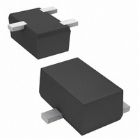
DDTA115GKA-7-F Diodes Inc, DDTA115GKA-7-F Datasheet

TRANS PREBIAS PNP 200MW SC59-3

DDTA115GKA-7-F

Manufacturer Part Number
DDTA115GKA-7-F
Description
TRANS PREBIAS PNP 200MW SC59-3
Manufacturer
Diodes Inc
Datasheet

Specifications of DDTA115GKA-7-F

Transistor Type
PNP - Pre-Biased
Current - Collector (ic) (max)
100mA
Voltage - Collector Emitter Breakdown (max)
50V
Resistor - Emitter Base (r2) (ohms)
100K
Dc Current Gain (hfe) (min) @ Ic, Vce
82 @ 5mA, 5V
Vce Saturation (max) @ Ib, Ic
300mV @ 500µA, 10mA
Frequency - Transition
250MHz
Power - Max
200mW
Mounting Type
Surface Mount
Package / Case
SC-59-3, SMT3, SOT-346, TO-236
Lead Free Status / RoHS Status
Lead free / RoHS Compliant
Mechanical Data
Maximum Ratings
Features
Collector-Base Voltage
Collector-Emitter Voltage
Emitter-Base Voltage
Collector Current
Power Dissipation
Thermal Resistance, Junction to Ambient Air (Note 1)
Operating and Storage Temperature Range
Notes:
DS30344 Rev. 8 - 2
DDTA114GKA
DDTA124GKA
DDTA144GKA
DDTA115GKA
Epitaxial Planar Die Construction
Complementary NPN Types Available (DDTC)
Built-In Biasing Resistor, R2 only
Lead Free/RoHS Compliant (Note 2)
"Green" Device Note 3 & 4
Case: SC-59
Case Material: Molded Plastic, "Green" Molding
Compound, Note 4. UL Flammability Classification
Rating 94V-0
Moisture Sensitivity: Level 1 per J-STD-020D
Terminals: Solderable per MIL-STD-202, Method 208
Lead Free Plating (Matte Tin Finish annealed over
Copper leadframe).
Terminal Connections: See Diagram
Marking Information: See Table Below & Page 3
Ordering Information: See Page 3
Weight: 0.008 grams (approximate)
P/N
1. Mounted on FR4 PC Board with recommended pad layout at http://www.diodes.com/datasheets/ap02001.pdf.
2. No purposefully added lead.
3. Diodes Inc.'s "Green" policy can be found on our website at http://www.diodes.com/products/lead_free/index.php.
4. Product manufactured with Date Code 0627 (week 27, 2006) and newer are built with Green Molding Compound. Product manufactured prior
to Date Code 0627 are built with Non-Green Molding Compound and may contain Halogens or Sb2O3 Fire Retardants.
R2 (NOM)
Characteristic
100KΩ
10KΩ
22KΩ
47KΩ
@T
A
= 25°C unless otherwise specified
Type Code
P26
P27
P28
P29
PNP PRE-BIASED SMALL SIGNAL SURFACE MOUNT TRANSISTOR
Schematic and Pin Configuration
www.diodes.com
K
J
IN
1 of 3
1
DDTA
B
A
G
H
T
Symbol
I
C
OUT
J
V
V
V
R
D
, T
3
(Max)
P
C
CBO
CEO
EBO
θ JA
Please click here to visit our online spice models database.
d
STG
R2
GND(+)
2
B C
E
L
(R2-ONLY SERIES)
-55 to +150
Value
-100
200
625
M
-50
-50
-5
DDTA (R2-ONLY SERIES) KA
All Dimensions in mm
Dim
M
A
B
C
D
G
H
K
J
L
α
0.013
SC-59
0.35
1.50
2.70
2.90
1.00
0.35
0.10
Min
© Diodes Incorporated
°C/W
Unit
mW
mA
°C
V
V
V
0.95
1.90
Max
0.50
1.70
3.00
3.10
0.10
1.30
0.55
0.20
KA

Related parts for DDTA115GKA-7-F

DDTA115GKA-7-F Summary of contents

Page 1

... Ordering Information: See Page 3 • Weight: 0.008 grams (approximate) P/N R2 (NOM) Type Code 10KΩ DDTA114GKA DDTA124GKA 22KΩ DDTA144GKA 47KΩ DDTA115GKA 100KΩ Maximum Ratings @T = 25°C unless otherwise specified A Characteristic Collector-Base Voltage Collector-Emitter Voltage Emitter-Base Voltage Collector Current Power Dissipation ...

Page 2

... Max Unit Test Condition ⎯ -50μA C ⎯ -1mA -720μA, DDTA114GKA -330μA, DDTA124GKA E ⎯ -160μA, DDTA144GKA -72μA, DDTA115GKA E μA -0 -50V CB -580 -260 μ -4V EB -130 -58 -0 -10mA -0.5mA C B ⎯ ⎯ -5mA - ⎯ +30 % ⎯ MHz V = -10V 5mA 100MHz ...

Page 3

... V , INPUT VOLTAGE (V) in Fig. 5 Collector Current vs. Input Voltage Ordering Information (Note 4 & 5) Device DDTA114GKA-7-F DDTA124GKA-7-F DDTA144GKA-7-F DDTA115GKA-7-F Notes: 5. For packaging details our website at http://www.diodes.com/datasheets/ap02007.pdf. Marking Information Date Code Key Year 2002 2003 Code N P Month Jan Feb Mar Code ...

Related keywords