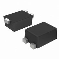
NSBC114EF3T5G ON Semiconductor, NSBC114EF3T5G Datasheet

NSBC114EF3T5G
Specifications of NSBC114EF3T5G
Related parts for NSBC114EF3T5G
NSBC114EF3T5G Summary of contents
Page 1
... Date Code Pb−Free Package ORDERING INFORMATION Device Package Shipping NSBC114EF3T5G SOT−1123 8000/Tape & Reel (Pb−Free) †For information on tape and reel specifications, including part orientation and tape sizes, please refer to our Tape and Reel Packaging Specifications Brochure, BRD8011/D. DEVICE MARKING INFORMATION See specific marking information in the device marking table on page 2 of this data sheet ...
Page 2
... Thermal Resistance Junction−to−Lead 3 (Note 1) Junction and Storage Temperature 2 1. FR−4 @ 100 oz. copper traces, still air FR−4 @ 500 oz. copper traces, still air. DEVICE MARKING AND RESISTOR VALUES Device Marking* NSBC114EF3T5G A (0°) NSBC124EF3T5G L (0°) NSBC144EF3T5G D (0°) NSBC114YF3T5G NSBC123TF3T5G T (0°) NSBC143EF3T5G P (0°) NSBC143ZF3T5G R (0° ...
Page 3
... NSBC144WF3T5G (BR)CBO V (BR)CEO NSBC114EF3T5G h FE NSBC124EF3T5G NSBC144EF3T5G NSBC114YF3T5G NSBC143EF3T5G NSBC143ZF3T5G NSBC123JF3T5G NSBC144WF3T5G = 10 mA 0.3 mA CE(sat NSBC114TF3T5G NSBC114EF3T5G NSBC124EF3T5G NSBC114YF3T5G NSBC123TF3T5G NSBC143EF3T5G NSBC143ZF3T5G NSBC123JF3T5G NSBC144EF3T5G NSBC144WF3T5G NSBC115TF3T5G http://onsemi.com 3 Min Typ Max Unit − − 100 nAdc − − 500 nAdc − ...
Page 4
... NSBC123TF3T5G/NSBC143ZF3T5G/NSBC114TF3T5G/ NSBC115TF3T5G Input Resistor Resistor Ratio NSBC114EF3T5G/NSBC124EF3T5G/ NSBC144EF3T5G/NSBC123EF3T5G NSBC114TF3T5G/NSBC115TF3T5G/NSBC123TF3T5G 4. Pulse Test: Pulse Width < 300 ms, Duty Cycle < 2.0 25°C unless otherwise noted) A Symbol Symbol = 1.0 kW NSBC114TF3T5G R1 NSBC114EF3T5G NSBC124EF3T5G NSBC144EF3T5G NSBC114YF3T5G NSBC123TF3T5G NSBC143EF3T5G NSBC143ZF3T5G NSBC123JF3T5G NSBC144WF3T5G NSBC115TF3T5G NSBC114YF3T5G NSBC143ZF3T5G NSBC123JF3T5G NSBC144WF3T5G http://onsemi.com ...
Page 5
... TYPICAL ELECTRICAL CHARACTERISTICS − NSBC114EF3T5G 1 25° 150° −55° COLLECTOR CURRENT (mA) C Figure 1. V vs. I CE(sat) 2.40 2.20 2.00 1.80 1.60 1.40 1.20 1.00 0. COLLECTOR BASE VOLTAGE (V) CB Figure 3. Output Capacitance 10 1.0 0. Figure 5. Input Voltage vs. Output Current ...
Page 6
TYPICAL APPLICATIONS FOR NPN BRTs +12 V FROM mP OR OTHER LOGIC Figure 6. Level Shifter: Connects Volt Circuits to Logic V CC OUT IN Figure 7. Open Collector Inverter: Inverts the Input Signal http://onsemi.com ISOLATED LOAD ...
Page 7
... H E *For additional information on our Pb−Free strategy and soldering details, please download the ON Semiconductor Soldering and Mounting Techniques Reference Manual, SOLDERRM/D. ON Semiconductor and are registered trademarks of Semiconductor Components Industries, LLC (SCILLC). SCILLC reserves the right to make changes without further notice to any products herein. SCILLC makes no warranty, representation or guarantee regarding the suitability of its products for any particular purpose, nor does SCILLC assume any liability arising out of the application or use of any product or circuit, and specifically disclaims any and all liability, including without limitation special, consequential or incidental damages. “ ...


