NSBA124EF3T5G ON Semiconductor, NSBA124EF3T5G Datasheet

TRANS DUAL PBRT PNP SOT-1123

NSBA124EF3T5G

Manufacturer Part Number
NSBA124EF3T5G
Description
TRANS DUAL PBRT PNP SOT-1123
Manufacturer
ON Semiconductor
Datasheet

Specifications of NSBA124EF3T5G

Transistor Type
PNP - Pre-Biased
Current - Collector (ic) (max)
100mA
Voltage - Collector Emitter Breakdown (max)
50V
Resistor - Base (r1) (ohms)
22K
Resistor - Emitter Base (r2) (ohms)
22K
Dc Current Gain (hfe) (min) @ Ic, Vce
60 @ 5mA, 10V
Vce Saturation (max) @ Ib, Ic
250mV @ 300µA, 10mA
Current - Collector Cutoff (max)
500nA
Power - Max
254mW
Mounting Type
Surface Mount
Package / Case
SOT-1123
Lead Free Status / RoHS Status
Lead free / RoHS Compliant
NSBA114EF3T5G Series
Digital Transistors (BRT)
PNP Silicon Surface Mount Transistors
with Monolithic Bias Resistor Network
device and its external resistor bias network. The digital transistor
contains a single transistor with a monolithic bias network consisting
of two resistors; a series base resistor and a base−emitter resistor. The
digital transistor eliminates these individual components by
integrating them into a single device. The use of a digital transistor can
reduce both system cost and board space. The device is housed in the
SOT−1123 package which is designed for low power surface mount
applications.
Features
Stresses exceeding Maximum Ratings may damage the device. Maximum
Ratings are stress ratings only. Functional operation above the Recommended
Operating Conditions is not implied. Extended exposure to stresses above the
Recommended Operating Conditions may affect device reliability.
MAXIMUM RATINGS
© Semiconductor Components Industries, LLC, 2008
September, 2008 − Rev. 2
Collector-Base Voltage
Collector-Emitter Voltage
Collector Current
This new series of digital transistors is designed to replace a single
Simplifies Circuit Design
Reduces Board Space
Reduces Component Count
The SOT−1123 Package can be Soldered using Wave or Reflow.
Available in 4 mm, 8000 Unit Tape & Reel
These are Pb−Free Devices
These are Halide−Free Devices
Rating
(T
A
= 25°C unless otherwise noted)
Preferred Devices
Symbol
V
V
CBO
CEO
I
C
Value
100
50
50
1
mAdc
Unit
Vdc
Vdc
†For information on tape and reel specifications,
NSBA114EFT5G
See specific marking information in the device marking table
on page 2 of this data sheet.
including part orientation and tape sizes, please
refer to our Tape and Reel Packaging Specifications
Brochure, BRD8011/D.
(INPUT)
BASE
PIN 1
DEVICE MARKING INFORMATION
Device
PNP SILICON DIGITAL
ORDERING INFORMATION
x
M
G or G
MARKING DIAGRAM
TRANSISTORS
http://onsemi.com
R1
R2
CASE 524AA
3
= Device Code
= Date Code
= Pb−Free Package
SOT−1123
SOT−1123
(Pb−Free)
STYLE 1
Package
x M
Publication Order Number:
1
1
(GROUND)
EMITTER
2
COLLECTOR
PIN 2
(OUTPUT)
8000/Tape & Reel
NSBA114EF3/D
PIN 3
Shipping

Related parts for NSBA124EF3T5G

NSBA124EF3T5G Summary of contents

Page 1

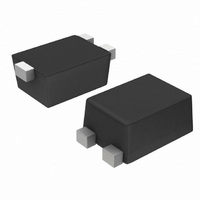
NSBA114EF3T5G Series Preferred Devices Digital Transistors (BRT) PNP Silicon Surface Mount Transistors with Monolithic Bias Resistor Network This new series of digital transistors is designed to replace a single device and its external resistor bias network. The digital transistor contains ...

Page 2

... FR−4 @ 100 oz. copper traces, still air FR−4 @ 500 oz. copper traces, still air. ORDERING INFORMATION, DEVICE MARKING AND RESISTOR VALUES Device Marking* NSBA114EF3T5G F (0°) NSBA124EF3T5G Y (0°) NSBA144EF3T5G E (0°) NSBA114YF3T5TG K (0°) NSBA123TF3T5G F (90°) NSBA143EF3T5G A (90°) NSBA143ZF3T5G E (90° ...

Page 3

... V E (BR)CBO V (BR)CEO NSBA114EF3T5G h FE NSBA124EF3T5G NSBA144EF3T5G NSBA114YF3T5TG NSBA143EF3T5G NSBA143ZF3T5G NSBA123JF3T5G NSBA144WF3T5G NSBA114TF3T5G = 10 mA 0.3 mA CE(sat NSBA114TF3T5G NSBA114EF3T5G NSBA124EF3T5G NSBA114YF3T5G NSBA123TF3T5G NSBA143EF3T5G NSBA143ZF3T5G NSBA123JF3T5G NSBA144EF3T5G NSBA144WF3T5G NSBA115TF3T5G = 1.0 kW http://onsemi.com 3 Min Typ Max Unit − − 100 nAdc − − 500 nAdc − ...

Page 4

... ELECTRICAL CHARACTERISTICS Characteristic Input Resistor Resistor Ratio NSBA114EF3T5G/NSBA124EF3T5G/ NSBA144EF3T5G/NSBA143EF3T5G NSBA114YF3T5TG NSBA123TF3T5G/NSBA114TF3T5G/ NSBA115TF3T5G NSBA143ZF3T5G NSBA123JF3T5G NSBA144WF3T5G (T = 25°C unless otherwise noted) (Continued) A Symbol NSBA114TF3T5C R1 NSBA114EF3T5G NSBA124EF3T5G NSBA144EF3T5G NSBA114YF3T5TG NSBA123TF3T5G NSBA143EF3T5G NSBA143ZF3T5G NSBA123JF3T5G NSBA144WF3T5G NSBA115TF3T5G http://onsemi.com 4 Min Typ Max Unit ...

Page 5

TYPICAL ELECTRICAL CHARACTERISTICS − NSBA114EF3T5G 1 25° COLLECTOR CURRENT (mA) C Figure 1. V vs. I CE(sat) 2.4 ...

Page 6

... H E *For additional information on our Pb−Free strategy and soldering details, please download the ON Semiconductor Soldering and Mounting Techniques Reference Manual, SOLDERRM/D. ON Semiconductor and are registered trademarks of Semiconductor Components Industries, LLC (SCILLC). SCILLC reserves the right to make changes without further notice to any products herein. SCILLC makes no warranty, representation or guarantee regarding the suitability of its products for any particular purpose, nor does SCILLC assume any liability arising out of the application or use of any product or circuit, and specifically disclaims any and all liability, including without limitation special, consequential or incidental damages. “ ...

Related keywords