MUN2111T1 ON Semiconductor, MUN2111T1 Datasheet
MUN2111T1
Specifications of MUN2111T1
Available stocks


Related parts for MUN2111T1

MUN2111T1 Summary of contents
Page 1
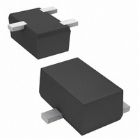
... MUN2111T1 Series Preferred Devices Bias Resistor Transistors PNP Silicon Surface Mount Transistors with Monolithic Bias Resistor Network This new series of digital transistors is designed to replace a single Bias Resistor Transistor (BRT) contains a single transistor with a monolithic bias network consisting of two resistors; a series base resistor and a base− ...
Page 2
... MUN2140T1 (Note 3) MUN2140T1G (Note 3) †For information on tape and reel specifications, including part orientation and tape sizes, please refer to our Tape and Reel Packaging Specifications Brochure, BRD8011/D. 3. New resistor combinations. Updated curves to follow in subsequent data sheets. MUN2111T1 Series Package Marking R1 (K) SC−59 ...
Page 3
... Output Voltage ( 1 1 1 1.0 kW Pulse Test: Pulse Width < 300 ms, Duty Cycle < 2.0%. MUN2111T1 Series = 25°C unless otherwise noted) A Symbol = CBO = CEO MUN2111T1 I EBO MUN2112T1 MUN2113T1 MUN2114T1 MUN2115T1 MUN2116T1 MUN2130T1 MUN2131T1 MUN2132T1 MUN2133T1 MUN2134T1 MUN2136T1 MUN2137T1 MUN2140T1 ...
Page 4
... Pulse Test: Pulse Width < 300 ms, Duty Cycle < 2.0%. 350 300 250 200 150 R = 370°C/W qJA 100 50 0 − AMBIENT TEMPERATURE (5°C) A Figure 1. Derating Curve MUN2111T1 Series (T = 25°C unless otherwise noted) A Symbol V OH MUN2111T1 MUN2112T1 MUN2113T1 MUN2114T1 MUN2133T1 MUN2134T1 MUN2136T1 MUN2137T1 MUN2130T1 MUN2115T1 MUN2116T1 MUN2131T1 ...
Page 5
... TYPICAL ELECTRICAL CHARACTERISTICS − MUN2111T1 −2°5C A 0.1 0. COLLECTOR CURRENT (mA) C Figure 3. V vs. I CE(sat REVERSE BIAS VOLTAGE (VOLTS) R Figure 5. Output Capacitance 100 0.1 0 Figure 7. Input Voltage vs. Output Current MUN2111T1 Series 1000 25°C 75°C 100 100 75° MHz 25° 0.1 0.01 ...
Page 6
... TYPICAL ELECTRICAL CHARACTERISTICS − MUN2112T1 0.1 0. COLLECTOR CURRENT (mA) C Figure 8. V vs. I CE(sat REVERSE BIAS VOLTAGE (VOLTS) R Figure 10. Output Capacitance 100 10 1 0.1 0 MUN2111T1 Series 1000 T = −25°C A 25°C 75°C 100 100 75° MHz 25° 0.1 0.01 0.001 Figure 11. Output Current vs. Input Voltage − ...
Page 7
... A 0.1 0. COLLECTOR CURRENT (mA) C Figure 13. V CE(sat) 1 0.8 0.6 0.4 0 REVERSE BIAS VOLTAGE (VOLTS) R Figure 15. Output Capacitance 100 10 1 0.1 0 MUN2111T1 Series 1000 25°C 75°C 100 vs 100 MHz 25° 0.1 0.01 0.001 Figure 16. Output Current vs. Input Voltage T = −25°C 25° ...
Page 8
... I , COLLECTOR CURRENT (mA) C Figure 18. V CE(sat) 4.5 4 3.5 3 2.5 2 1 REVERSE BIAS VOLTAGE (VOLTS) R Figure 20. Output Capacitance 10 1 0.1 0 Figure 22. Input Voltage vs. Output Current MUN2111T1 Series 180 160 CE 140 25°C 120 75°C 100 vs 100 MHz 25° INPUT VOLTAGE (VOLTS) in Figure 21 ...
Page 9
... I , COLLECTOR CURRENT (mA) C Figure 23. V vs. I CE(sat REVERSE BIAS VOLTAGE (V) R, Figure 25. Output Capacitance 10 1 0.1 0 Figure 27. Input Voltage vs. Output Current MUN2111T1 Series 1000 100 25°C 75° Figure 24. DC Current Gain C 100 75° MHz 25° 0.01 0. Figure 26. Output Current vs. Input Voltage T = − ...
Page 10
... I , COLLECTOR CURRENT (mA) C Figure 28. V versus I CE(sat REVERSE BIAS VOLTAGE (VOLTS) R Figure 30. Output Capacitance 75°C 0.1 0 Figure 32. Input Voltage versus Output Current MUN2111T1 Series 1000 75°C 100 25° 100 75° MHz 25° 0 −25°C A 0.01 0.001 Figure 31. Output Current versus Input Voltage = − ...
Page 11
... I , COLLECTOR CURRENT (mA) C Figure 33. Maximum Collector Voltage vs. Collector Current 1.2 1.0 0.8 0.6 0.4 0 REVERSE BIAS VOLTAGE (VOLTS) R Figure 35. Output Capacitance 100 25° Figure 37. Input Voltage vs. Output Current MUN2111T1 Series 1000 100 75°C 25° 100 MHz 25° 0 Figure 36. Output Current vs. Input Voltage T = − ...
Page 12
... COLLECTOR CURRENT (mA) C Figure 38. Maximum Collector Voltage vs. Collector Current 1.4 1.2 1.0 0.8 0.6 0.4 0 REVERSE BIAS VOLTAGE (VOLTS) R Figure 40. Output Capacitance 100 10 25° Figure 42. Input Voltage vs. Output Current MUN2111T1 Series 1000 75°C 100 Figure 39. DC Current Gain 100 MHz 25° ...
Page 13
... Literature Distribution Center for ON Semiconductor P.O. Box 5163, Denver, Colorado 80217 USA Phone: 303−675−2175 or 800−344−3860 Toll Free USA/Canada Fax: 303−675−2176 or 800−344−3867 Toll Free USA/Canada Email: orderlit@onsemi.com MUN2111T1 Series PACKAGE DIMENSIONS SC−59 CASE 318D−04 ISSUE G NOTES: 1 ...