LMN200B01-7 Diodes Inc, LMN200B01-7 Datasheet
LMN200B01-7
Specifications of LMN200B01-7


Related parts for LMN200B01-7


LMN200B01-7 Summary of contents
Page 1
... LOAD SWITCH FEATURING PRE-BIASED PNP TRANSISTOR AND N-MOSFET General Description LMN200B01 is best suited for applications where the load needs to be turned on and off using control circuits like micro-controllers, comparators, etc., particularly at a point of load. It features a discrete pass transistor with stable ...
Page 2
... Drain Current (Page 1: Note 3) Continuous (V Pulsed (tp <10 uS, Duty Cycle <1%) Continuous Source Current DS30651 Rev Symbol Value V -50 CBO V -50 CEO V - -200 unless otherwise specified A Symbol V DSS V DGR V GSS = 10V www.diodes.com = 25 C unless otherwise specified A Unit Value Unit +/-20 V +/-40 115 mA 800 115 mA LMN200B01 ...
Page 3
... I = -100 A -0 -5V -0.05V -50V -500 - -50mA -5mA -0 -0 -20mA -1mA -100mA -10mA -200mA -10mA -200mA -20mA -0 -200mA -10mA 1 -5V - -5V - -5V -100 -5V -200 -0.3V -5V, = -2.5V -50mA /-2.5mA -5V - -5V -200mA -1 -50mA -5mA -3 -80mA -8mA -5 -10V -5mA MHz f = 100MHz V = -10V 0A 1MHz LMN200B01 ...
Page 4
... T , AMBIENT TEMPERATURE (°C) A Fig. 3, Max Power Dissipation vs Ambient Temperature www.diodes.com Unit Test Condition =0V 60V 20V -20V 0.25mA 5V 50mA 10V 115mA 10V DS(ON 5V 50mA 10V 500mA 115 mA DS DS(ON 200 mA DS DS(ON -25V 0V 1MHz 30V, V =10V 200mA 150 0V 115 mA 175 LMN200B01 ...
Page 5
... 100 I , COLLECTOR CURRENT (mA) C Fig vs www.diodes.com 125° -55° 150° 25° 85° COLLECTOR CURRENT (A) C Fig vs. I CE(SAT -55° 25° 150° 125° 85° 100 1000 I , COLLECTOR CURRENT (mA) C Fig vs. I BE(ON) C 150°C 1000 LMN200B01 ...
Page 6
... GATE-SOURCE VOLTAGE (V) GS Fig. 10 Transfer Characteristics Pulsed T = 125° 150° 85° 25° -55°C A 0.01 0.1 I DRAIN CURRENT ( Fig. 12 Static Drain-Source On-Resistance vs. Drain Current T = 25°C A Pulsed I = 115mA GATE SOURCE VOLTAGE (V) GS, Fig. 14 Static Drain-Source On-Resistance vs. Gate-Source Voltage LMN200B01 ...
Page 7
... T = 125° 150° 25° 85° Pulsed 0 SOURCE-DRAIN VOLTAGE (V) SD Fig. 16 Reverse Drain Current vs. Source-Drain Voltage T = -55° 25° 85° 125° 150°C A 0.2 0.4 0.6 0 DRAIN CURRENT (A) D Fig. 18 Forward Transconductance vs. Drain Current (V > DS(ON) LMN200B01 Diodes Incorporated ...
Page 8
... Application Details PNP Transistor (DDTB142JU) and N-MOSFET (DSNM6047) with gate pull-down resistor integrated as one in LMN200B01 can be used as a discrete entity for general purpose applications integrated circuit to function as a Load Switch. When it is used as the latter as shown in Fig 19, various input voltage sources can be used as long as it does not exceed the maximum ratings of the device ...
Page 9
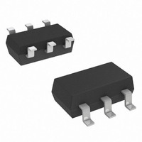
... Ordering Information (Note 5) Device LMN200B01-7 Note: 5. For Packaging Details our website at http://www.diodes.com/datasheets/ap02007.pdf. Marking Information PM1 Fig. 21 Date Code Key Year Code Month Jan Feb Code 1 2 DS30651 Rev Marking Code Packaging PM1 SOT-26 PM1 = Product Type Marking Code Date Code Marking ...
Page 10
... M J 0.013 0.35 M 0.1 0 All Dimensions in mm Figure 23 Dimensions IMPORTANT NOTICE LIFE SUPPORT www.diodes.com SOT-26 Max Typ 0.5 0.38 1.7 1 0.55 3.1 3 0.1 0.05 1.3 1.1 0.55 0.4 0.2 0.15 8° - SOT-26* 3.2 1.6 0.55 0.8 2.4 0.95 LMN200B01 ...